
MicroLEDs with a size less than about 10 ?m x 10 ?m are needed to fabricate high resolution microled based microdisplays. Unfortunately, it has been found that the performance of microleds in this size range tend to suffer from sidewall defects. The presence of such defects decreases external quantum efficiency and increases power consumption. The good news is that Atomic Layer Deposition (ALD) can be used to address the sidewall defect problem by growing a passivation layer on microleds.
This Display Daily article relates to the subject of microled passivation and draws upon research conducted by a team headed by An-Chen Liu of the National Yang Ming Chiao Tung University (Taipei City, Taiwan) and utilizing ALD equipment made by Picosun OY (Espoo, Finland). A recent article on this subject by the team is entitled “Increase in the Efficiency of III-Nitride microleds: Atomic-Layer Deposition and Etching.” It was published in IEEE Nanotechnology Magazine, vol. 15, no. 3, PP 18-34 and is available on-line for purchase by typing the name of the article into your browser.
First a few words of somewhat detailed background information.
Degradation in microleds derives from surface recombination and sidewall deterioration of the microled mesas. The degradation is caused by one of the device fabrication steps, the plasma assisted dry etching process used for chip isolation. The nature of the sidewall degradation is the generation of defects on the mesas that act as active sites for nonradiative recombination. Since the luminous efficiency of LEDs depends on the competition between radiative and nonradiative recombination, the increase in nonradiative recombination results in a reduction in light extraction efficiency. Shockley-Read-Hall and Auger recombination are considered the two main forms of nonradiative recombination. The extent of the Shockley-Read-Hall recombination grows as the size of the microled decreases due to an increase in the density of surface states.
ALD is an effective approach to address sidewall defects because it is capable of depositing a highly compact dielectric film with nanometer scale thickness. Further advantages of using ALD are that it allows precise control the film thickness, deposits pinhole free thin films and provides excellent step coverage.
The figure below was obtained with a scanning electron microscope and is of a layer of dielectric Al2O3 deposited on a sidewall by atomic layer deposition.
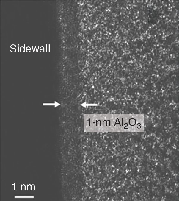 An image obtained with a scanning electron microscope of a layer of Al2O3 deposited on a sidewall using ALD.
The ALD equipment and procedures used to fabricate a variety of prototype devices as well as the means used to measure device properties is described thoroughly in the IEEE article. An additional technology investigated and also reported in the article relates to the use of atomic layer etching as an additional means to improve microled performance. Atomic layer etching can provide excellent depth control in shallow device structures.
A few of the top level results are as follows. III-nitride microleds of different sizes were fabricated with and without ALD deposited Al2O3 passivation. The results showed external quantum efficiency enhancement of 70% for 5 µm x 5 µm microleds and 60% for 10 µm x10 µm microleds when using ALD Al2O3 passivation.
The researchers also report on a second advantage to the use of ALD in microled devices. It applies when inkjet printing is used to pattern quantum dots as a means to achieve a full color display. In this case, Picosun ALD passivation technology was successfully used to minimize the effects of photo-oxidation and consequent degradation of quantum dot performance. It was reported that, after a 500 hours environmental reliability test, the color gamut “remained at an excellent level.”
The team concludes their article with the assessment that ALD and atomic layer etching techniques have been shown to effectively mitigate defects in microleds and prevent performance degradation in microled based devices. -Arthur Berman
Picosun, Juhana Kostamo, +358-50-369-9565