
The paper that I stumbled upon concerns the development of polysilicon in large substrates for OLEDs or LCDs. Those that have been in the industry some time can skip the next brief introduction for those that don’t know what polysilicon is or does.
Allotropes of Silicon
Silicon can exist in various crystal forms, known by scientists as allotropes. Another example of a material with a number of allotropes is carbon. If we ignore buckminsterfullerene and some more exotic forms, the simplest for carbon are probably soot, which has no crystal structure, graphite which has layers (which is why it is slippy – the layers move easily) and diamonds which are very dense and hard. They are all carbon, but the atoms are differently arranged.
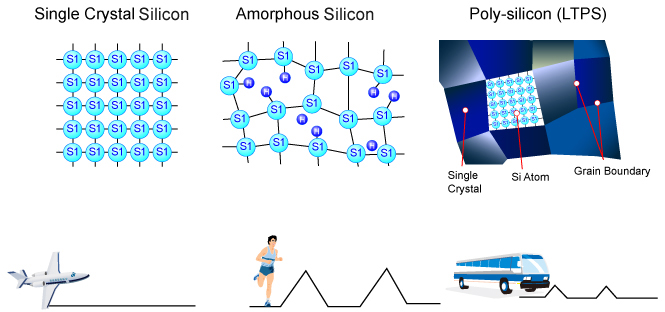 Image:National Formosa University
In the same way, silicon can be amorphous (like soot), polysilicon (with some structure, but grain boundaries) and crystal silicon (which is used to make silicon chips). The different structures make it easier for electrons to move quickly through the material as you go from amorphous to crystal.
On the back of most LCDs, the silicon used for the transistors is amorphous silicon. That’s a shame, as better silicon allows the performance to be improved, for example with smaller transistors that work faster and with lower power. It has to be amorphous silicon that is deposited because the melting point of silicon is higher than the melting point of the glass that the silicon is deposited on, so you would expect that melting and re-crystallising the silicon would damage the substrate.
LTPS Comes Along
So, someone had the idea of using a very fast blast of laser energy to just melt the surface of previously deposited amorphous silicon, so that it would re-crystallise as polysilicon. That worked and enabled the concept of Low Temperature Polysilicon (LTPS) to be developed. As a result, LCD makers were able to make better and better displays, with high pixel density and with drive circuitry integrated on the panel itself improving reliability and reducing cost. LTPS effectively enabled high quality LCDs for smartphones and were essential for small OLED displays, as the transistor configuration is much more complicated than for LCDs.
Now, LTPS was developed a long time ago. However, there were limitations in the way it was done. One was the cost. The laser equipment has a limited life and is expensive, so you have to be making relatively expensive displays. Also, it is very tricky to get the polysilicon to re-crystallise evenly over large areas, so, as far as I know, the largest ever mass production LTPS panel was a 32″ panel made by TM Displays and used in an OCB LCD TV panel back in 2004. Again, as far as I know, this panel, which was very expensive (but very good) was only used by Eizo to make TVs in Japan. The difficulty of making large LTPS substrates was one of the reasons for the failure of Samsung’s project to make large RGB OLEDs for TV. While Samsung chose LTPS as its transistor system for large OLEDs, LG Display chose oxide.
G6 Has Been the Limit
So, the largest LTPS fabs in the world are at G6 (unless a reader knows differently!) which would mean that they are designed for displays up to 37″ or so and a substrate size around 1.5m x 1.8m. This is because the height of the laser system has to be very accurately controlled to keep the laser focussed and that has proved difficult at larger sizes. More recent G6 fabs have been for making small OLEDs, especially flexible displays. LTPS would be a big advantage for high frame rate 8K LCDs as well as for other emissive displays that need better transistors.
A Surprise in the Symposium Digest
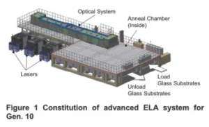
Anyway, while looking through the SID Symposium digest, I was surprised to spot a paper presented by ‘The Japan Steel Works’ of Yokohama, that describes how the firm has developed a news Excimer Laser Annealing (ELA) system for large substrates up to G10.

The firm has developed a new transport system for the process which reduces the time between substrates when processing in pairs, so that the overall processing time is reduced – making the TACT time lower and increasing the throughput. The system uses a ‘floating area’ based on gas, to keep the surface of the substrate at a precise distance from the laser system. It has made mass productions with a G6.1 scale already, using a 1,000mm line length, but the firm claims that it can be extended to 1,500mm, currently the state of the art in ELA.
You can see from the picture above that given that the G10 glass substrates are over 3 metres wide, the equipment would be very large indeed.
Customers Needed
The firm, of course, will need a customer ready to commit to the technology to get LTPS into a G10 fab. That may be tricky for LCD makers that are not looking for technology risk, and probably wouldn’t want to consider the cost of ELA in their panels. However, in LCDs, the transistor only ‘operates the tap’ rather than needing to deliver the energy needed to light the pixel. That energy comes from the backlight in an LCD. In emissive displays, which could be QD OLED, QNED or microLED, all the energy goes through the TFTs, so you need really good transistors to keep them efficient. Being able to make LTPS at G10 could be a significant help to those looking to develop TV-sized emissive displays. (BR)
(Of course, there has been a huge amount of work been put in to use Oxides such as IGZO instead of silicon to allow better transistor performance without the need for crystallisation, but that’s a topic for another day!)