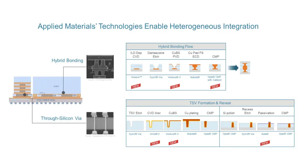
Applied Materials has introduced a range of materials, technologies, and systems that enable chipmakers to integrate chiplets into advanced 2.5D and 3D packages using hybrid bonding and through-silicon vias (TSVs). These new solutions expand Applied Materials’ comprehensive suite of technologies for heterogeneous integration (HI), addressing industry challenges arising from the increasing demand for transistors in applications like high-performance computing and artificial intelligence.
Heterogeneous integration allows semiconductor companies to combine chiplets with different functions, technology nodes, and sizes into advanced packages, enabling them to function as a single product. This approach overcomes the limitations of traditional 2D scaling, which no longer delivers simultaneous improvements in performance, power, and cost. HI, therefore, plays a vital role in enhancing chip performance, power efficiency, cost-effectiveness, and time to market (PPACt).
By incorporating more transistors and wiring in 2.5D and 3D configurations, these new HI solutions enhance system performance, reduce power consumption, minimize size, and accelerate time to market. HI has a number of potential benefits for display manufacturing, including:
- Increased functionality: HI can be used to integrate different types of functionality into a single display, such as touch sensing, image processing, and communication. This can lead to more powerful and versatile displays.
- Reduced power consumption: HI can be used to reduce the power consumption of displays by integrating different types of devices that can be turned on and off as needed. This can be especially beneficial for mobile devices, where power consumption is a major concern.
- Reduced cost: HI can be used to reduce the cost of displays by integrating different types of devices that can be manufactured in the same process. This can save on manufacturing costs and lead to more affordable displays.
However, HI also has some challenges, including:
- Complexity: HI can be a complex process, and it requires the use of advanced packaging technologies. This can make it difficult and expensive to implement.
- Compatibility: HI requires that the different types of devices that are being integrated are compatible with each other. This can be a challenge, as different devices often have different requirements.
- Testing: HI can be difficult to test, as it requires testing of the different types of devices that are being integrated. This can add to the cost of HI.