One of the more profound papers on core microdisplay (MD) technology advancement at SID Display Week came from a Columbia University start-up company, Lumiode. In Session 26.2 the team led by Dr. Brian Tull presented the paper ‘High Brightness Emissive Microdisplay by Integration of III-V LEDs with Thin Film Silicon Transistors’. The group hopes to deliver an emissive device with megapixel addressable sizes and multi-kilolumen output from its LED Light engine. This is a microdisplay based on type III-V compound semiconductor materials optimized for optoelectronic devices. The goal is nothing less than a fundamental change in technology to create a high brightness emissive LED MD using thin film transistors. This is a photolithographically pixelated LED used as both the light source and the image component. In essence, we are talking about large signage LEDs shrunk down to the micro display size.
To Tull, the demand for wearables and micro devices is driving the need to move away from traditional micro displays including spatial light modulators (SLM), LCD, or digital micro-mirror (DMDs) that require a separate light source. Further, he contends the emissive OLED option lacks sufficient light output for truly wearable applications and daylight readability. OLED simply cannot compete with its cousin, the inorganic compound based LEDs. To Tulls point: “LEDs offer the brightest (20M cd/m²), highest efficacy (100 lm/W), and most robust (50,000 hours) controllable light source,” he said.
LEDs Based on Type III-V Compound Semiconductor Material
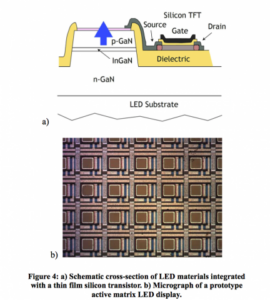
To get there, the team first uses photolithography to pattern optimized LED materials into arrays using traditional tools and patterning techniques to achieve sub micron resolutions. Tull said this approach is also scalable to high volumes. The group fabricates the LED array (first) then deposits a thin film of amorphous silicon that is laser crystallized to form the active transistor layer. This approach “…provides an extremely local, surface-contained, high temperature process which melts and crystallizes the silicon on the surface, leaving the underlying LED layers near room temperature,” according to Tull. It’s a tried and true method used both in LCD glass substrate and OLED display manufacturing. Tull emphasized, “Our transistor process flow follows a conventional thin film process with several modifications to ensure process compatibility with LED epitaxial wafers.” The final step is to monolithically integrate the thin film device with standard GaN-based LEDs, and the group has developed a combined process flow.
The science of combining new materials such as type III and V compound semiconductors is opening some amazing application areas in the display space. The technology promises advantages in brightness, efficiency, and overall system size reduction to meet the needs of the next generation wearable micro display devices. The Lumiode technology may well serve as a case in point, but as always, time will tell. – Steve Sechrist
For another initiative in this space, check our video interview with Ostendo (Ostendo Shows Impressive Microdisplays)