Thin Film Transistors (TFTs) are typically produced using one of three processes: amorphous silicon, low temperature polysilicon or indium gallium zinc oxide. New research suggests that there is an opportunity to replace and improve upon these processes.

Target applications include the production of the TFTs used to drive pixels in active matrix displays sized from large liquid crystal and OLED displays to microLED displays.
The new, non-laser technology is being developed by a team of researchers from Solar-Tectic LLC (Briarcliff Manor, NY), Blue Wave Semiconductors Inc. (Baltimore, MD), the Center for Autonomous Solar Power and the Department of Electrical and Computer Engineering at Binghamton University (Binghamton, NY).
A recent article on the technology is entitled “High mobility crystalline silicon film growth below 600°C from an Au-Si eutectic melt for TFTs.” It was published in the journal Materials Letters, Volume 219, 15 May 2018, Pages 138-142. A copy of the article is available for purchase on-line. It can be found here.
The team reported on the growth of a crystalline silicon thin film on buffered soda lime glass below 600?°C from a gold – silicon eutectic melt.
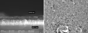
The team characterized the film using x-ray diffraction, x-ray photoelectron spectroscopy, Raman spectroscopy, transmission electron microscopy and cross section scanning electron microscopy.
Images of the film are presented in the figure below.
Images of the thin film.
Characterization methods confirmed a thin a continuous film of highly crystalline silicon had been grown on the buffered soda lime glass. Electron mobility was found to be 188?cm²?/Vs as determined using a Hall Effect-based measurement. This mobility value is higher than those typically reported for either low temperature polysilicon or indium gallium zinc oxide.
The new eutectic enhanced recrystallization process can reportedly take place at a temperature as low at 232°C when using tin as the metal with silicon. The process is quite different from Metal Induced Crystallization because there is no metal residue left in the silicon film and the insulator layer is crystalline which allows for heterogeneous nucleation of silicon.
Solar-Tectic has reported plans to make samples using its newly patented insulator layer in conjunction with highly oriented “textured” MgO crystals. The company believes that this could lead to even higher electron mobility. In addition, Solar-Tectic has stated the intention to soon start a pilot line to “deliver certain types of components for use in various industrial applications.” -Arthur Berman
Solar-Tectic, Ashok Chaudhari, [email protected]
For more on the commercial aspects of this development, see Ken’s DD interview with Solar-Tectic (Team Develops a Backplane Material Better than LTPS)