A team of researchers led by Professor Kyoung-Duck Park of the Department of Physics within the Ulsan National Institute of Science and Technology (Ulsan, Republic of Korea) is developing a novel means of controlling the brightness and wavelength of light emitted by quantum dots.

Previous research has established that the application of strain to nanoscale level materials such as perovskite quantum dots (pQDs) can enable tuning of their optoelectronic properties over a wide range. Up to now, however, manipulation at the single emitter level has never been attempted. Recent work by the team focused on addressing this issue.
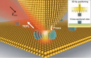
The approach investigated by the team was based on tip-induced dynamic control of strain, bandgap and quantum yield of single CsPbBrxI3–x pQDs. The specific means by which this was implemented included a controllable plasmonic nanocavity in conjunction with so-called Tip-Enhanced PhotoLuminescence (TEPL) spectroscopy.
A recent article by the team on this topic is entitled “Tip-Induced Strain Engineering of a Single Metal Halide Perovskite Quantum Dot.” It was published in ACS Nano 2021, 15, 5, 9057-9064. A copy of the article is available for purchase and can be found here.
Paraphrasing this article: based on the results of their experiments, the team was able to report that single CsPbBrxI3–x pQDs were clearly resolved by the use of hyperspectral TEPL imaging with ?10 nm spatial resolution. The plasmonic tip was then used to directly apply pressure to a single pQD. The result was a bandgap shift up to ?62 meV. This, in turn, resulted in a Purcell enhanced photoluminescence increase as high as ?105. (Note: the Purcell effect is the enhancement of a quantum system’s spontaneous emission rate by virtue of its environment.) Furthermore, by systematically modulating the tip-induced compressive strain applied to a single pQD, the team demonstrated dynamical bandgap engineering in a reversible manner. In addition, they facilitated quantum dot coupling of a pQD ensemble by the use of ?0.8 gigapascal tip pressure at the nanoscale.
A graphic illustrating the experimental set up is presented in the figure below.
 Graphic illustration of the experimental setup.
Two top level conclusions were drawn and reported based on the research results. The first was that extremely high tip-induced local pressure allowed pressure induced recrystallization and phase transition at a length scale of a few nanometers. As a consequence, the approach was represented as a possible means to further improve the grain quality and optical properties of 2D perovskite ensembles as a post fabrication process. Second, that the extrinsically modified physical properties of pQDs accomplished by adjusting the plasmonic cavity could significantly improve the efficiency of perovskite photovoltaics.
In their article, the team included the comment that their new approach offers a practical way to tune the mechanical and electronic properties at the single pQD level for potential applications in ultra-compact nano-optoelectronic devices. More specifically, that dynamical single dot manipulation should be able to enable nano-LEDs and, thus, realize ultra-high definition, high efficiency displays.
The team concluded their article with the general statement that “Our approach presents a strategy to tune the nano-opto-electro-mechanical properties of pQDs at the single crystal level.” -Arthur Berman
Ulsan National Institute of Science and Technology, Kyoung-Duck, [email protected]