This week’s news contained a report that, for the first time, OLED electrodes have been produced from graphene.
The process was developed and optimized as part of an EU-funded program called the “Gladiator” project. The more formal name for the project is Graphene Layers: Production, Characterisation and Integration. Partners in this project are The Fraunhofer Institute for Organic Electronics, Electron Beam and Plasma Technology FEP (Dresden, Germany), Graphenea S.A. (San Sebastián, Spain) and Aixtron Ltd. (Cambridge, United Kingdom). The project leader is Fraunhofer’s Dr. Beatrice Beyer.
Graphene consists of a single layer of carbon atoms in which the atoms are arranged in a honeycomb-like pattern. A layer of graphene is only 0.3 nanometers thick. Graphene is a particularly interesting material because it is light, transparent, extremely hard and has greater tensile strength than steel. In addition, it is flexible and highly conductive of both heat and electricity.
One of the challenges in producing graphene, especially as a transparent electrode, is how to achieve homogenous coverage over a large area. The approach utilized in the Gladiator project is based on CVD equipment provided by Aixtron. The production of the graphene electrodes for OLED’s is the responsibility of Graphenea.
The production process takes place in a steel vacuum chamber in which a plate of high purity copper is heated to about 800 degrees C. A mixture of methane and hydrogen gas is then introduced into the chamber. Upon injection, a chemical reaction is initiated in which the methane dissolves in the copper depositing carbon atoms on the surface of the plate. Only a few minutes are required to cover the entire surface of the plate.
A Gladiator press release explained that “the production process was optimized using new diagnostic and process control instrumentation based on Raman spectroscopy and spectrometric ellipsometry.”
The extent of the graphene layer is expanded beyond the size of the CVD tool by implementing an innovative “patchwork” process. In this process, the first step is to allow the plate to cool. A carrier polymer is then placed on the graphene and the copper plate is etched away.
After the transfer, the quality of graphene layers is assured using “new noncontact inline eddy current measurements and THz imaging.”
This transfer process is reported to have “a high yield and negligible impact upon the properties of the graphene.”
The process under development is expected to be appropriate for use in organic large area electronics in which the substrate and barrier properties have been specifically optimized for use with graphene. In addition, the transfer process will be developed for both rigid and flexible substrates.
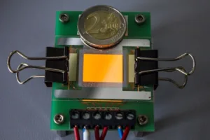
At this time, electrodes have been produced having dimensions of 2cm x 1cm. The illustration below is of an orange, luminous OLED on a graphene electrode.
The researchers anticipate that CVD production costs per unit area can be reduced. Means that will be investigated to achieve this goal include process parameter optimization, development of methods to re-use the catalysts and by increasing the size of the reactor chamber.
Beyer stated that the first products using the new technology could become available in two to three years. In considering such products, she noted that, due to their flexibility, graphene electrodes are well suited not only for use in displays but also in touch screens, photovoltaics and high-tech textiles.
The Fraunhofer team is currently working on minimizing impurities and defects which occur during the transfer of the graphene thin film to another carrier material. The Gladiator project is funded through April, 2017. -Arthur Berman
Fraunhofer COMEDD, Beatrice Beyer, [email protected]