In Super Twisted Nematic LCs, we see how multiplexed addressing allows an array of pixels to be controlled in such a way as to allow a high definition display to be built with liquid crystals. The method used to switch individual pixels in multiplexed displays, called passive matrix addressing, has many drawbacks, such as:
- Current leakage among adjacent pixels causes ghosting, or “crosstalk”, and reduces contrast;
- Because of the high twist angles of the liquid crystal, viewing angles are limited;
- Response times for the high twist angles are also slow. This causes smearing of moving image elements, such as a mouse pointer.
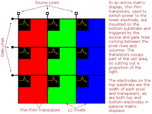
In the late 1960’s, an alternative to passive addressing was developed which uses a thin film diode in the corner of each LC pixel on the rear backplane of the two glass substrates which make up the LCD sandwich. The thin film diode was later replaced by a thin film transistor (TFT), which proved more efficient. Although the presence of the opaque TFT within each cell boundary means that a brighter back light is required with this addressing method, current leakage between the top and bottom substrates is reduced because of the isolation provided by the transistor. Moreover, because the transistor controls the charge on the LC material, a conventional twisted nematic alignment can be used, reducing smearing and making the display of motion video possible for the first time. The finer control also allows a number of variations in LC material and cell configuration to address the problems of ensuring wider viewing angles. This method of driving an LC matrix is called Active Matrix (AM) addressing and AM LCD panels have become the most commonly used in notebook computers, desktop monitors and video projectors.
However, the more complex AM design, which provides more opportunities for manufacturing faults and raises production costs, took a long time to become a commercial proposition and it wasn’t until the mid- to late-1980’s that the first 2″ AM TFT LCDs appeared in portable colour TVs. In the meantime, work continued on passive matrix displays, with new techniques, such as dual-scanning of STN displays (known as DSTN) providing sufficient improvements to the basic design to persuade researchers that it was worth persevering with the cheaper technology. Dual-scanning portions the display into an upper and lower half with each section driven by independent column drivers.
Update: Active matrix LCDs are now the displays of choice for all notebook, desktop monitor and TV applications. They are now being increasingly used in mobile phone applications as the desire to show motion video becomes more important. Larger displays for notebooks, monitors and TVs generally use transistors made of amorphous silicon, which is relatively easy to make at low temperatures, but has low electron mobility. Small TFT displays are often made using polysilicon for the transistors in the substrate. These are more efficient and allow the integration of drivers and other circuitry, but are more difficult to make.
The idea of using an active or passive matrix backplane has been applied to OLEDs, ePaper and other display applications. At the time of writing (July 2006), active matrix OLEDs are being made by just one company for commercial applications in mobile phones. Active matrix OLEDs are usually made with polysilicon transistors although research and development work is being undertaken to make amorphous silicon active matrix OLEDs.

