Vuzix, the maker of Augmented Reality smart glasses, is working with Plessey Semiconductor and Jasper Display to create a new display device to drive their AR smart glasses.
The development roadmap calls for monochrome devices this summer and full color by the end of the year. That could mean a new smartglass product would become available in 2019.
According to the developers, the microLED light engine would be about half the size of competitive solutions and would be very bright and power efficient – all the right attributes for a next generation AR display.
At CES 2019, we had a chance to see an early monochrome prototype that was a hand-held waveguide with the microLED display as the source. The image was visible in daylight.
Plessey Semiconductor is a UK-based company that is using GaN-on-Silicon technology to create monolithic microLED microdisplays. Plessey (like Allos Semiconductor and Aledia) believe that fabricating on silicon has huge advantages especially in terms of size, mature tooling, scaling and cost. GaN-on-sapphire is limited to 6”, but Plessey’s GaN-on-Silicon wafers can be made up to 10 inches in diagonal.
Plessey acquired the GaN-on-silicon technology from Cambridge University in 2012 and in 2013 introduced a 6” wafer for LED development across a range of market segments. As the size of the wafer increases, there is the chance for the hybrid wafer to warp or “potato chip” due to strain. Plessey says it has solved this problem and part of the solution is to go to a planar LED structure.
Plessey Can Make Efficient Small Devices
In a technical paper at SID DisplayWeek, Keith Strickland said the firm has made microLED devices down to as small as 1 micron. And, they have seen the external quantum efficiency (EQE) exceed 20% on devices as small as 4 microns. This last is actually a big deal. EQE decreases dramatically as the size of the LED gets smaller and smaller, often in the low single digits for devices this small. (This seems to be because of edge defects and a lot of work by researchers including LETI in France is going on to improve the performance of small devices – Man. Ed.)
To make a microLED, Plessey has teamed up with Jasper Display. Jasper has made LCOS microdisplays for some time but in recent years has been offering its backplane technology as a platform for other uses. One of them is for microLEDs. (Jasper Display Optimistic About MicroLED Potential – subscription required).
Jasper modified the backplane a bit to create current drivers for the microLEDs vs. voltage drivers needed for LCOS. Modifications include adding more metal on the top to cope with current of up to two amps. Individual pixels can support currents from 0.2µA to 1.0µA. The backplane is fabricated in the usual way in a conventional CMOS foundry.
Plessey is then responsible for fabricating the microLEDs on their GaN-on-Silicon wafer. Strickland says that using a silicon substrate not only allows larger and more economical processing compared to sapphire, but it allows for better LED devices too. How so, we asked?
He described the key GaN-on-Silicon technology advantages as:
- Better thermal performance (lower LED operating temperature = higher reliability)
- Focused light-emitting surface
- Uniformity
For example, did you know the thermal conductivity of silicon is 6X better than sapphire? (Thermal conductivity of silicon =149 W/(m•K) vs. Thermal conductivity of sapphire =27 W/(m•K))
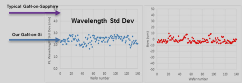
In terms of wavelength uniformity, the data below shows the standard deviation of their GaN-on-Silicon solution vs. a GaN-on-sapphire solution. However, such uniformity is very equipment and process dependent, so comparisons may not be that helpful. The second data set shows low bowing in the hybrid wafer over a number of wafers.
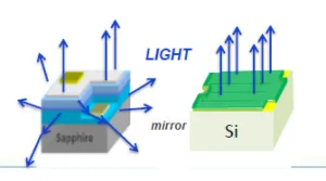
The focused light comes from the planar structure with mirror.
Plessey fabricates the microLEDs as a planar structure with N and P contacts on the top surface along with a mirror layer over the active area. This hybrid wafer is then flipped over and mated to the CMOS backplane creating a structure with microLEDs and active matrix sandwiched between two silicon wafers. The final step is the remove the silicon wafer from the GaN-on-silicon side to reveal the microLEDs.
These steps are not as simple as they sound. There is considerable IP involved in aligning two opaque silicon wafers, in the contacting materials, in planarity, and in silicon wafer removal. All this must be done with high yields and good time efficiency.
To support Vuzix, Plessey plans to use the Jasper SP70 backplane, which is a 0.7” diagonal device with 1920 x 1080 pixels on a 8 micron pixel pitch capable of 60 fps operation. The monochrome (blue) version should be delivered this summer.
To get to full color, Plessey plans to use a RGGB pattern over this same display with red and green quantum dots deposited at this 8 micron pitch. The blue sub-pixel would have nothing over it. No details on partners or process were disclosed, however. This remains an area of development as well. The result will be a full color display with 960 x 540 resolution. This is scheduled to be available by the end of 2018.

A Gen II display is planned for June 2019. This will be a 1” diagonal device with 1920 x 1080 resolution and 60 fps operation with a 11.5 full-color pixel pitch. Plessey says the display architecture will be a triad arrangement so it may include some sub-pixel rendering (the sub-pixel pitch is 5.8 microns). DeepSky is also working on a triad microLED architecture which uses subpixel rendering to try to improve resolution. – CC