
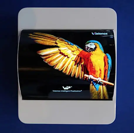
At the 2023 World Ultra High Definition Video Industry Development Conference the company unveiled its Visionox intelligent pixelization technology (ViP). Essentially, ViP technology combines photolithography techniques with AMOLED display manufacturing, removing any application of fine metal mask (FMM) processes. The company claims that ViP boosts the aperture ratio of AMOLED from a conventional 29% to a staggering 69%, and will allow for pixel densities over 1700 ppi. When paired with Visionox’s tandem OLEDs, ViP could result in six times the lifespan, or four times the brightness, of standard FMM AMOLEDs.
Replacing FMM with photolithography eliminates color mixing and crosstalk between subpixels at low brightness further enhancing AMOLED clarity, color performance, and uniformity. ViP also brings a new layer of refinement to mature FMM AMOLED technologies, such as tandem OLEDs, bio-sensors, and under-screen cameras. For example, without any design alterations or cost increases, ViP technology can double the transmission rate of under-screen sensors compared to what may be achieve with the FMM process, creating new opportunities for under-screen camera technology.
Anticipating demand in the mid-to-large size AMOLED panel market, Visionox had begun construction of a ViP production line in its Hefei location back in 2022 and building out volume capabilities. Additionally, Visionox has filed patents across multiple domains, including photolithographic pixel patterning, auxiliary cathodes, independent OLED devices, and independent packaging. As of now, Visionox boasts nearly a hundred core patents.
FMM and Photolithography
FMM technology has been a vital part of AMOLED manufacturing, facilitating the deposition of organic materials onto the substrate. However, FMM technology has some limitations that become increasingly evident as display requirements advance:
- Resolution Limitations: FMM struggles to meet the high-resolution requirements of modern devices. As pixel densities increase (especially beyond 500ppi), the mask’s metal patterns become too fine and prone to deformation during the deposition process, reducing yield.
- Size Limitations: FMM is less suitable for large-sized panels. As the size of the display grows, the mask must also grow, making it susceptible to bending or warping, which can impact the accuracy of deposition and overall display quality.
- Production Efficiency: The FMM process is time-consuming and complex, impacting the efficiency of mass production.
- Cost: The masks used in FMM are expensive to produce and maintain, adding to the overall production cost.
Photolithography, on the other hand, is a well-established technique used in the semiconductor industry that has several advantages over FMM:
- Higher Resolution: Photolithography can precisely define smaller features, enabling much higher pixel densities, thereby improving the resolution of the display.
- Greater Uniformity and Precision: Photolithography ensures better uniformity and precision of the deposited layers, which can enhance the performance and lifespan of the AMOLED panels.
- Scalability: Unlike FMM, photolithography is not constrained by the size of the panel, making it suitable for larger displays.
- Production Efficiency: Photolithography is a more streamlined and efficient process, making it better suited for high-volume manufacturing.
- Cost: While photolithography equipment is a significant investment, it can be more cost-effective in the long run due to its efficiency, precision, and scalability.