VerLASE Technologies announced today that the US Patent Office has issued US Patent No. 9,035,344 on a novel wavelength conversion technology based on Quantum Wells (QWs) formed from exfoliated 2D materials.
 Immediate applications include solid state lighting (SSL) and displays of all kinds, ranging from large flat panel displays to smaller smartphone and tablet screens, offering a practical way around some of the technical hurdles pacing broader adoption of Quantum Dots (QDs) and traditional phosphors for color conversion. The technology can be further extended with different material sets into IR and UV ranges for a variety of other applications.
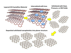
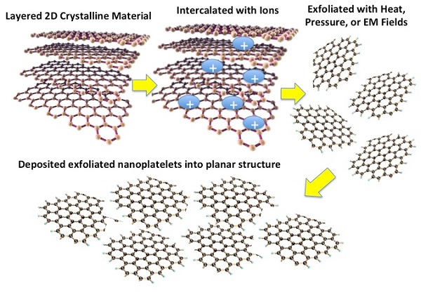
Semiconducting 2D materials like Graphene have captured a great deal of attention for their huge potential in numerous applications. Such materials grow in crystalline layers weakly bound to each other, like sheets in a ream of paper, and can be readily exfoliated into extremely thin layers. VerLASE had been investigating photoluminescent QWs made from nanoplatelets of such materials as Gallium Selenide, Tungsten Disulfide, and Moly Disulfide, among others. When excited (for example with low cost blue LEDs), these materials can re-emit or downconvert light into colors otherwise difficult to obtain (particular Reds, Greens and Yellows). They are quantum confined structures directly analogous to QDs but are “flat,” 2D structures, and can be used similar to how QDs are currently being used for color conversion.
The photoluminescence of a QW depends on its material composition and thickness, just like the downconverted color of a QD depends on material and dot size. QWs also offer similar optical advantages with narrower spectral characteristics, better colors and color saturation when compared to traditional phosphors, but in sharp contrast to QDs, QWs of 2D materials offer much better thermal characteristics, a significant challenge with QDs and traditional phosphors in many lighting, projector and display applications. Moreover, 2D materials have minimal dangling bonds, so are inherently self-passivated. They are more stable emitters, without the blinking and non-reversible photobleaching disadvantages of QDs.
Exfoliated sheets of 2D semiconductor materials may also be used “as they are,” sandwiched by air or another higher bandgap material, or they can be encased by wider bandgap semiconductor materials. The sheet of 2D material in the middle then forms the “Well” region. VerLASE shows how QWs of 2D materials can be made inexpensively by the exfoliating 2D crystals grown in a furnace. Such exfoliation can be done in multiple ways, including chemically by intercalating certain ions between the layers of a 2D crystal, then breaking the crystal apart into its constituent layers in the form nanoplatelets of uniform thickness.
These exfoliated, anisotropic 2D nanoplatelets can then be deposited in a preferential “flat” orientation. VerLASE has demonstrated a proprietary R2R method for laying down such 2D nanoplatelets using a modified Langmuir Blodgett technique. Other approaches are possible, for example, embedding the 2D nanoplatelets in a polymer matrix with 1D, 2D stretching. Color converting sheets can be made at very low cost for ease of integration into other applications. For example, an add-on red-emitting phosphor sheet can be readily made to create “warm white” light in a conventional SSL luminaire. Gallium Selenide QW nanoplatelets with emission in the 610-620 nm range and a bandwidth of 30-40 nm are ideally suited.
QDs in commercial products to date have been limited to passive, optically pumped color converters, despite a vision that they could be made inexpensively in a beaker, then combined with P- and N- doped semiconductors to form low cost, electroluminescent devices; however, various technical and economic hurdles have stood in the way. “We believe the unique attributes of 2D QW nanoplatelets can enable the original QD vision of electroluminescent devices,” explained Ajay Jain, VerLASE’s Chief Technical Officer and inventor of the technology, adding that same basic 2D semiconductor materials can also be used as Gain Media for lasers and other high value electro-optical devices.