Researchers in Denmark recently achieved a significant development in the field of integrated photonics and quantum technologies with the experimental creation of an indium phosphide (InP) nanocavity. This nanocavity boasts an exceptionally small mode volume of 0.26 (λ/2n)^3, surpassing the previous records by more than tenfold for III-V semiconductor nanocavities and quadrupling the diffraction limit’s capabilities. The crucial aspect of this innovation is the intense spatial confinement of light within the semiconductor, significantly boosting the radiative emission rate through the Purcell effect. This advancement paves the way for the development of nanoscale lasers and LEDs, potentially achieving the ultra-small active regions required for single-emitter applications.
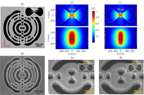
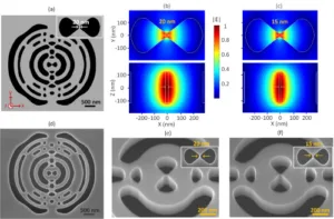
The design and creation of two InP nanocavities, named TO-EDC g20 and TO-EDC g15, featuring central dielectric bridge widths of 20 nm and 15 nm respectively, illustrate this achievement. Utilizing topology optimization to navigate fabrication constraints, the design showcases a bowtie-like structure facilitating light confinement at a narrow dielectric bridge. The sophisticated nanoscale features were crafted using electron beam lithography and optimized dry etching, with the optical properties assessed experimentally. Techniques like cross-polarized confocal microscopy and near-field scanning optical microscopy (s-SNOM) verified the high Q-factors and extreme light confinement, closely aligning with simulations.
The nanocavities’ compact and efficient light sources hold significant potential for on-chip optical interconnects, sensing, and the enhancement of single-photon emitters like quantum dots or color centers. This is critical for on-demand single-photon sources in quantum information processing, quantum key distribution, and quantum metrology, fostering the exploration of fundamental quantum electrodynamics phenomena and applications in quantum gates, switches, and memories. Furthermore, the broadband nature of Purcell enhancement and the high field intensities could revolutionize nonlinear optical processes and spectroscopic sensing, offering new avenues for efficient frequency conversion, all-optical switching, and enhanced signal detection from nanoscale analytes.
In display technology, these nanocavities could revolutionize MicroLED pixels by reducing power consumption and increasing modulation speeds, essential for high-resolution VR and AR applications. By enabling narrow-band color conversion through the integration of different emitters, displays could achieve unprecedented color gamut, saturation, and efficiency. The potential for integration with CMOS electronics and other photonic components promises compact, high-resolution microdisplays and advanced display systems with enhanced performance and functionalities.
Despite the promising applications, the journey from experimental realization to practical devices involves addressing scalability, uniformity, electrical injection, and packaging challenges. However, the extreme light confinement demonstrated in these InP nanocavities marks a significant step towards next-generation display technologies and the broader application of integrated photonics and quantum technologies.
Reference
Xiong, M., Christiansen, R. E., Schröder, F., Yu, Y., Casses, L. N., Semenova, E., Yvind, K., Stenger, N., Sigmund, O., & Mørk, J. (2024). Experimental realization of deep sub-wavelength confinement of light in a topology-optimized InP nanocavity. Optical Materials Express, 14(2), 397–406. https://doi.org/10.1364/OME.513625