In recent years, I have been more and more convinced of the need for a mid-performance semiconductor in the display industry. While amorphous silicon (a-Si) is the industry workhorse and covers almost 60% of the display industry by value, its capabilities are limited in some cases: it is not uniform enough, and not stable enough to be used by OLED and it is not always capable enough to drive 8K displays or high density displays at high refresh rates.

LTPS on the other hand, is too expensive and too unwieldy to be used for large panel markets, with its requirements for ELA (excimer laser anneal) and doping and high mask count. Hence the need for a mid-performance, “easy to manufacture” semiconductor. Higher mobility semiconductors mean
- greater pixel density at high frame rates,
- typically higher current capability which can mean higher brightness in OLED
- the option for lower power
- the option for integrated functionality such as row and column multiplexing or memory in pixel
- slimmer form factors with narrower bezels and
- integrated value (such as Fingerprint/Haptics and Speaker on Display [FOD, HOD and SOD] from Samsung Display [SDC]).
IGZO theoretically fills that role. It is a mid-performance semiconductor with typical mobility of 15-20 cm²/Vs in mass production. However, IGZO is a challenging technology where the semiconductor layer itself often needs to be protected by an etch stop layer (ESL) to stop interaction with the surrounding layers. Only a small handful of players have truly mastered the technology, including LG Display (LGD) and Sharp. Many players have tried but have found the technology challenging to implement.
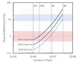
We have talked about the benefits above, but these are further reinforced by the graph shown in Figure 1, which shows higher frame rates and higher density displays require higher mobility. And IGZO today is the basis and fundamental starting point of large panel emissive technologies, such as LGD’s WOLED and SDC’s QD OLED displays and CSOT’s IJP OLED display.
 Figure 1. Required TFT mobility as a function of number of pixels in a display. Adapted from [1].
Players in the arena have repeatedly made calls for the need for higher performing IGZO. Every year at SID there are a broad range of papers looking at new approaches to increasing IGZO performance. This article presents a review that one of our clients made of the different ways that IGZO mobility can be increased, as we believe that this is a topic that has not had its day in mainstream discussion. Their review, shown in Table 1, is based on the search terms “High performance IGZO” in SID Journals and Technical Digests from Jan 2018 – March 2021, specifically looking at differing mechanisms for IGZO mobility enhancement.
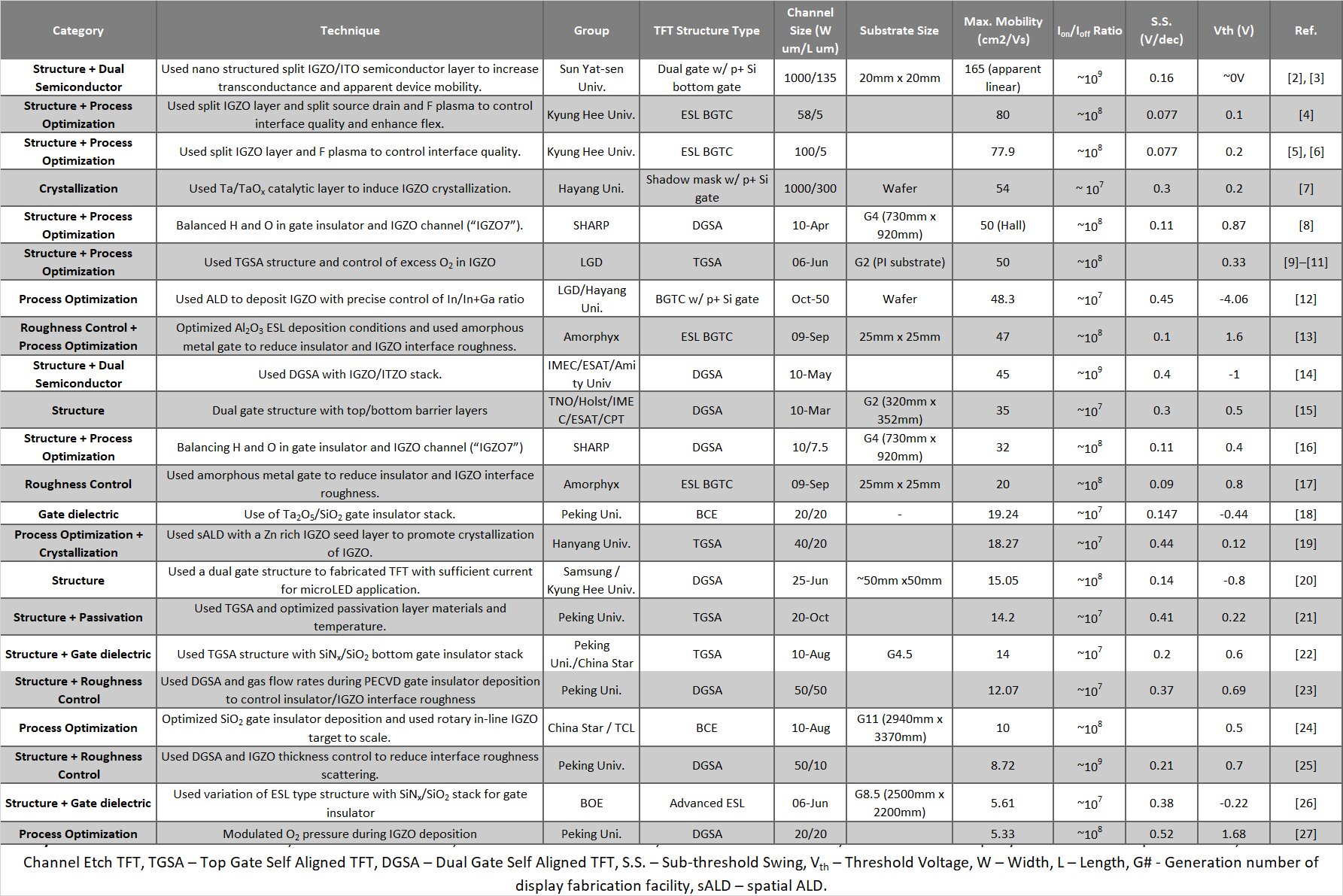 Table 1. Device data for IGZO based TFTs found by a search of “high+mobility+IGZO” in “Journal of the Society for Information Display” or “SID Symposium Digest of Technical Papers” from Jan 2018 to March 2021 (approximately 247 results returned). Click for higher resolution or download the Excel below.
You can download the table as an XL file here.![]() Research_Table.xlsx
Research_Table.xlsx
Six Approaches
Six common approaches to improving mobility have been identified from the data shown in Table 1.
Approach 1 is Process optimisation and is the most common. Process optimization can be realized by subtly adjusting hydrogen and oxygen flows during depositions or switching to alternate deposition methods
Approach 2 is to use more complex TFT structures. Dual gate coplanar and top gate self-aligned structures have been used and do successfully increase mobility, if modestly. Split channel TFTs as an approach can make a big difference to mobility, but come at the cost of larger TFT footprints and have yet to be proven on large area substrates.
Approaches 1 and 2 are the most common place ideas from the big display players
Approach 3 is to use some form or other of crystallisation method. In the search performed for this article the most common method is a thin-film “catalyst” layer, but excimer laser annealing, such as that is used for LTPS, has also been proposed. While these methods may work, it heads down the direction of increased process cost (just like LTPS). If we want a mid-performance semiconductor, then we want it without the need for crystallisation
From the research, the new frontier seems to be the use of the following three new ideas:
Approach 4 is to use dual layers of IGZO and related materials in the semiconductor layer. In the early days there was lots of work done on attempts to optimise the constituent weights within the IGZO composition but that now seems to have given way to bilayer constructions, such as IGZO with ITZO. This work is promising, but may or may not lead to additional masks and sputter steps in production
Approach 5 is to change the TFT gate and/or passivation dielectric. Here a range of materials have been used from silicon nitride/oxide stacks to tantalum or aluminium oxides. The goal is generally to reduce leakage current for gate dielectrics and improve moisture barrier capability for passivation layers, while avoiding harmful interactions of either with IGZO. Aluminium oxide ends up being a pretty decent option in this regard given its low leakage current and low water permeability, plus its ability to play well with IGZO.
Approach 6 is to control the roughness of gate insulator and IGZO interfaces and thereby reduce interface trap states and scattering of carriers in the channel. This can be achieved by improving deposition conditions, reducing IGZO thickness or by using amorphous metal gates to enable thinner Al2O3 gate dielectrics and thinner IGZO channels.
What is interesting is that these approaches are broadly additive since they have different mechanisms. Players can try to use process optimisation, with a new structure with dual layer semiconductors and at the same time deploy a dielectric/passivation approach and optimise surface roughness. With these, perhaps in combination, we may yet see IGZO TFT reaching the levels of LTPS but without the ELA and doping.
My client, which is Amorphyx, that did all this intellectual analysis for us, has some pretty good ideas on the use of dielectrics/passivation layers and roughness control as two levers as part of their IGZO amorphous metal TFT (AMeTFT) approach. If you are interested, go talk to them. They have shown high mobilities (of 60 cm²/Vs and higher) for a simple ESL type TFT using their smooth amorphous metal gate to influence the surface roughness and aluminium oxide gate dielectric/passivation to improve stability. They are now focusing on further improvements through alternative TFT structures, such as dual gate.
Better performing mid-tier semiconductors are needed by the market to help deliver higher functionality in the large panel sexy emissive displays of the future. There are only a limited number of real approaches when looking at IGZO enhancement, as we have tried to show, and perhaps this sets out a roadmap for better IGZO based displays in the future. (Ian Hendy)
Ian Hendy is a Display Stategy Consultant based in London, UK. Hendy Consulting provides growth strategy, technology strategy and deal/M&A assessments for players throughout the display value chain. Amorphyx is a client of Hendy Consulting.
Thanks to Amorphyx Inc for releasing this article outside the subscription system which means that it does not count towards your free allocation of articles.
References
[1] T. Kamiya, K. Nomura, and H. Hosono, “Present status of amorphous In–Ga–Zn–O thin-film transistors,” Science and Technology of Advanced Materials, vol. 11, no. 4, p. 044305, Feb. 2010, doi: 10.1088/1468-6996/11/4/044305.
[2] K. Huang, Z. Chen, S. Hu, L. Gao, and C. Liu, “31-2: Invited Paper: Nanostructures Oxide Thin-Film Transistors Fabricated by Near-Field Nanolithography with Enhanced Device Performance,” SID Symposium Digest of Technical Papers, vol. 51, no. 1, pp. 448–451, 2020, doi: https://doi.org/10.1002/sdtp.13901.
[3] K. Huang et al., “Nanostructured High-Performance Thin-Film Transistors and Phototransistors Fabricated by a High-Yield and Versatile Near-Field Nanolithography Strategy,” ACS Nano, vol. 13, no. 6, pp. 6618–6630, Jun. 2019, doi: 10.1021/acsnano.9b00665.
[4] S. Lee, Y. Chen, J. Kim, H. Kim, and J. Jang, “Highly robust oxide TFT with bulk accumulation and source/drain/active layer splitting,” Journal of the Society for Information Display, vol. 27, no. 8, pp. 507–513, 2019, doi: https://doi.org/10.1002/jsid.823.
[5] S. Lee, Y. Chen, J. Kim, H.-M. Kim, and J. Jang, “Transparent AMOLED display driven by split oxide TFT backplane,” Journal of the Society for Information Display, vol. 26, no. 3, pp. 164–168, Mar. 2018, doi: 10.1002/jsid.646.
[6] S. Lee, D. Geng, L. Li, M. Liu, and J. Jang, “Highly robust oxide thin film transistors with split active semiconductor and source/drain electrodes,” in 2017 IEEE International Electron Devices Meeting (IEDM), Dec. 2017, p. 8.2.1-8.2.4, doi: 10.1109/IEDM.2017.8268350.
[7] Y. Shin, S. T. Kim, and J. K. Jeong, “24.2: Invited Paper: High Mobility Oxide Thin-Film Transistors on Basis of a Microstructure Modification,” SID Symposium Digest of Technical Papers, vol. 49, no. S1, pp. 252–254, 2018, doi: https://doi.org/10.1002/sdtp.12694.
[8] K. Ito et al., “24-1: Invited Paper: Development of High Quality IGZO-TFT with Same On-Current as LTPS,” SID Symposium Digest of Technical Papers, vol. 51, no. 1, pp. 343–346, 2020, doi: https://doi.org/10.1002/sdtp.13874.
[9] D. H. Kim et al., “5-2: Gate Driver Circuits for Internal Compensation Type OLED Display with High Mobility Oxide TFT,” SID Symposium Digest of Technical Papers, vol. 49, no. 1, pp. 40–43, May 2018, doi: 10.1002/sdtp.12486.
[10] J. U. Bae et al., “High mobility oxide TFT for OLED pixel circuits,” in 2017 24th International Workshop on Active-Matrix Flatpanel Displays and Devices (AM-FPD), Jul. 2017, pp. 309–311.
[11] J. U. Bae et al., “10.2: Invited Paper: Development of Oxide TFT’s Structures,” SID Symposium Digest of Technical Papers, vol. 44, no. 1, pp. 89–92, 2013, doi: https://doi.org/10.1002/j.2168-0159.2013.tb06148.x.
[12] M. H. Cho et al., “P-13: High Performance a-IGZO Thin-Film Transistors Grown by Atomic Layer Deposition: Cation Combinatorial Approach,” SID Symposium Digest of Technical Papers, vol. 50, no. 1, pp. 1259–1262, 2019, doi: https://doi.org/10.1002/sdtp.13162.
[13] S. W. Muir, D. R. Kearney, and J. E. Mendez, “A Novel Pixel Control Circuit Containing Non-linear Resistors and Thin Film Transistors for Active Matrix Flat Panel Displays,” SID Symposium Digest of Technical Papers, vol. 52, no. S1, p. 58, 2021, doi: https://doi.org/10.1002/sdtp.14373.
[14] M. Nag et al., “P-12: High Performance Dual-gate Dual-layer Amorphous Oxide Semiconductors TFTs on PI Foil for Display Application,” SID Symposium Digest of Technical Papers, vol. 50, no. 1, pp. 1255–1258, 2019, doi: https://doi.org/10.1002/sdtp.13161.
[15] A. J. Kronemeijer et al., “P-127: Dual-Gate Self-Aligned IGZO TFTs Monolithically Integrated with High-Temperature Bottom Moisture Barrier for Flexible AMOLED,” SID Symposium Digest of Technical Papers, vol. 49, no. 1, pp. 1577–1580, 2018, doi: https://doi.org/10.1002/sdtp.12311.
[16] Y. Takeda et al., “37-2: Development of high mobility top gate IGZO-TFT for OLED display.,” SID Symposium Digest of Technical Papers, vol. 50, no. 1, pp. 516–519, 2019, doi: https://doi.org/10.1002/sdtp.12970.
[17] D. R. Kearney, J. E. Mendez, S. R. Self, J. P. Anderson, and S. W. Muir, “P-196: Late-News-Poster: Low-Temperature All Sputter IGZO-TFT Fabricated with Amorphous Metal Thin-Films,” SID Symposium Digest of Technical Papers, vol. 51, no. 1, pp. 1400–1403, 2020, doi: https://doi.org/10.1002/sdtp.14148.
[18] Z. Wang, Y. Hu, Q. Lin, L. Li, and K.-C. Chang, “Performance Improvement of a-IGZO Thin-Film Transistor By Using Ta2O5/SiO2 Double-layer Gate Dielectric,” SID Symposium Digest of Technical Papers, vol. 51, no. S1, pp. 1–3, 2020, doi: https://doi.org/10.1002/sdtp.13736.
[19] H. Seul, H. Yang, N. On, and J. K. Jeong, “P-7: Highly-Ordered Indium-Gallium-Zinc Oxide Thin Film Transistor via Atomic Layer Deposition Process.,” SID Symposium Digest of Technical Papers, vol. 50, no. 1, pp. 1237–1240, 2019, doi: https://doi.org/10.1002/sdtp.13156.
[20] J.-W. Choi et al., “30-5: Late-News Paper: Glass-based High brightness AMLED using Dual Gate Coplanar a-IGZO TFT,” SID Symposium Digest of Technical Papers, vol. 51, no. 1, pp. 440–443, 2020, doi: https://doi.org/10.1002/sdtp.13899.
[21] X. Zhang, X. Deng, H. Yang, L. Zhang, and S. Zhang, “P-1.6: Effect of Deposition Condition of Passivation Layer on the Performance of Self-Aligned Top-Gate a-IGZO TFTs,” SID Symposium Digest of Technical Papers, vol. 49, no. S1, pp. 535–537, 2018, doi: https://doi.org/10.1002/sdtp.12774.
[22] Q. Ma, X.-Y. Zhou, Y.-J. Hsu, Y.-C. Wu, and S.-D. Zhang, “Excellent Uniformity and Reliability Top-Gate Self-Aligned IGZO TFTs with Cu Electrode,” SID Symposium Digest of Technical Papers, vol. 51, no. S1, pp. 184–186, 2020, doi: https://doi.org/10.1002/sdtp.13785.
[23] L. Qin, X. Deng, J. Tao, and S. Zhang, “P-1.14: The Influence of Bottom gate Dielectric Roughness on the Performance of Double-Gate a-IGZO Thin Film Transistors,” SID Symposium Digest of Technical Papers, vol. 50, no. S1, pp. 677–680, 2019, doi: https://doi.org/10.1002/sdtp.13608.
[24] H.-S. Seo et al., “21-3: Invited Paper: High Quality 8K4K Displays driven by Oxide Semiconductor Thin Film Transistor in the Generation 11 Equipment,” SID Symposium Digest of Technical Papers, vol. 51, no. 1, pp. 301–304, 2020, doi: https://doi.org/10.1002/sdtp.13863.
[25] X. Zhang, X. Deng, H. Yang, X. Zhou, L. Zhang, and S. Zhang, “P-13: Electrical Characteristics and Stability of Double-Gate a-IGZO Thin Film Transistors with Self-Aligned Top-Gate,” SID Symposium Digest of Technical Papers, vol. 49, no. 1, pp. 1227–1230, 2018, doi: https://doi.org/10.1002/sdtp.12131.
[26] F. Shang et al., “P-6: Development of Advanced Etch-Stop Structures Oxide TFT,” SID Symposium Digest of Technical Papers, vol. 49, no. 1, pp. 1212–1214, 2018, doi: https://doi.org/10.1002/sdtp.12102.
[27] X. Deng, X. Zhang, T. Liang, X. Zhou, and S. Zhang, “P-1.14: The Influence of Dual-channel on the Performance of Self-Align Top-Gate IGZO Thin Film Transistors,” SID Symposium Digest of Technical Papers, vol. 49, no. S1, pp. 561–564, 2018, doi: https://doi.org/10.1002/sdtp.12782.