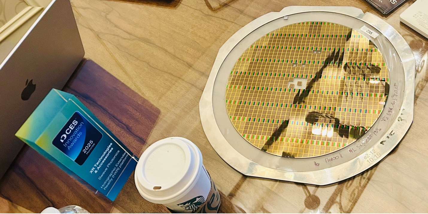
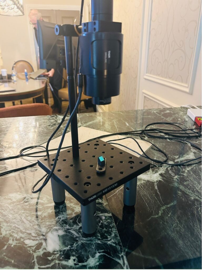
Swave Photonics hit the news just before CES with a Series A raise of €27 million ($28.27 million), money earmarked for “enabling a reality-first user experience for AI-powered augmented reality (AR) smart glasses and heads-up displays,” the company says. We met with them in Las Vegas to hear the latest.I’ve known Swave Photonics’ CEO Mike Noonen on and off over the years, starting at NXP and then GlobalFoundries, so I was very interested when he joined Swave Photonics, a company tackling spatial computing using nanopixel holography.
Wait, what?! Well, it took Mike about 1 minute into our first meeting to conjure up the Princess Leia hologram from Star Wars as an inspiration.
Swave’s Holographic Extended Reality (HXR) technology utilizes the smallest pixels available to manipulate light and create 3D holographic images for interactive and environment-aware UX. The technology is meant to enable the human visual system to naturally process images through a patented technology.
Current AR devices face several challenges, notably visual issues like vergence-accommodation conflict, which can lead to nausea or fatigue for users. Swave’s HXR technology should address those problems, while also eliminating the need for expensive components like waveguides or varifocal lenses, which are typically necessary for existing AR devices.
So, Princess Leia?
Mike Nooen: Holography often feels like one of those ‘flying car’ technologies—the future everyone expects but never quite arrives. The perception is heightened with holography because we’ve been watching it in movies for 50 years, starting with iconic images like Princess Leia in Star Wars. But the reality is that holography as a science was invented 75 years ago by Dennis Gabor. He was working at a TV company outside London when he created the photographic process for holograms. At the time, that was the only way to achieve the precision required for holography.
We’re now advancing holography into the digital age by creating the world’s first legitimate holographic displays. We’ve broken through the ‘sound barrier’ of pixel pitch. It’s not about being pedantic or on a quixotic mission to educate the world about holography. However, we do want to clear up misconceptions.
That’s necessary because most people picture the Princess Leia hologram without understanding the technical dependencies.
Noonen: Exactly. That’s okay because a rising tide lifts all boats. But what we’re doing is fundamentally different from other technologies, and for good reason. This isn’t just about the technology; it’s about the cycles of learning. Historically, photonics hasn’t advanced much since Galileo’s time. The field has relied on grinding glass, but now it’s moving toward siliconization and tunability. We’re bringing semiconductor processes and cycles of learning to photonics, leveraging a half-trillion-dollar industry. We’re a fabless photonics company—a category that didn’t even exist three years ago.
Congratulations on your recent Series A. It seems people are beginning to see the potential here. What’s changed?
Noonen: The AR/VR and Metaverse market has consumed and destroyed more wealth than almost any other sector. Companies with deep pockets have been throwing money at physics problems, trying to force breakthroughs. For example, Meta made significant investments in Bristol to get Plessey to push gallium nitride beyond its capabilities, and Apple has worked extensively with ams Osram. Despite these efforts, the story repeats: established technologies are pushed to their limits, but true breakthroughs often come from entirely new directions.
This is where innovators’ dilemmas come into play—technology comes from an unexpected vector and disrupts conventional wisdom. We’re not claiming to be as transformative as, say, the disk drive industry, but we’re pushing the boundaries of what’s possible in photonics. The industry is moving toward siliconization, and we’re at the forefront, thanks to a significant head start provided by Imec. They began exploring holographic displays a decade ago using legacy display technology, but their pixel pitch—even at state-of-the-art levels—was an order of magnitude too large. We’ve solved that problem.

Scaling down pixel size seems to be a universal challenge in photonic computing, whether it’s for AI or displays. How did you manage it?
Noonen: Once we solved the pixel pitch issue, it had a cascade of benefits. No one will catch up to us because we have a 12-year head start. Achieving this breakthrough required us to think beyond traditional materials, leveraging the entire periodic table. I like to describe it as the photonic equivalent of a Reese’s Peanut Butter Cup: phase-change material and display technology coming together.
To create true holography—interference of light waves forming a 3D image in free space—you need an extremely wide field of view. Achieving this requires pixel spacing smaller than half the wavelength of light. Legacy display technologies like DLP or liquid crystal on silicon just can’t scale down enough. When pixels are larger than the light you’re trying to steer, you disrupt it rather than control it.
Can legacy technologies create usable holograms at all?
Noonen: They can, but the field of view is so narrow that the images are impractical. This is why technologies like waveguides exist—to replicate and expand the image for usability. However, waveguides are inefficient intermediaries. For example, even the best waveguides have only about 1% efficiency. By eliminating the need for waveguides, everything improves: cost, efficiency, weight, and complexity.
Our platform, Holographic Extended Reality (HXR), includes a chipset based on two major breakthroughs. First, we developed a tiny pixel using phase-change material. This material is well understood, bistable, and can change its optical properties quickly and without power. Second, we’ve created a system for real-time holographic image generation that doesn’t require supercomputers.

Is the primary application for glasses or HUDs?
Noonen: We’re starting with glasses, but the technology is scalable. It could be used in windshields, TVs, or even holographic walls. We’re already working with customers on applications like 3D TVs without glasses and advanced heads-up displays (HUDs).
HUDs seem like a market where legislation might drive adoption. What’s the right technology to make it happen?
Noonen: Exactly. HUDs are an ideal application for holography. While we initially thought autonomous driving would reduce the need for HUDs, the opposite is true. Since Level 5 autonomy is still far off, drivers need critical information presented clearly and intuitively. Our technology can do that by placing information exactly where it belongs in the real world.
What’s the road map for your technology?
Noonen: We’ll debut our dynamic chip at SID Display Week in May. This prototype will be the world’s first holographic display chip, featuring 250 million pixels. Early customers will test it, provide feedback, and help us refine the design for production tape-out by year-end. Our chips are fabricated using standard 22 nm processes, leveraging mainstream semiconductor infrastructure. This keeps costs low—we’re targeting $50 per eye for the entire system, which is orders of magnitude less expensive than other holographic solutions.
That’s incredible. Is there a dependency on laser technology?
Noonen: No, we’re using existing low-cost laser technology. While there’s room for innovation in light sources, our platform is already compatible with today’s lasers, making it practical and cost-effective.
Your cost targets seem transformative compared to other holographic technologies. Most of them are talking about systems costing tens of thousands of dollars.
Noonen: That’s the difference between being in the semiconductor ecosystem versus the traditional photonics ecosystem. By leveraging standard semiconductor processes, we achieve scalability and cost efficiency that bespoke photonics solutions can’t match.

Over a 30-year career in technology marketing and communications, David Harold has pushed GPU boards for ATI, Matrox, and VideoLogic, and IP for Imagination Technologies. He’s been “in the room” for some of the most exciting developments in GPU and gaming. He’s now helping start-ups in cleantech, edutech, and semiconductors, with strategy, marketing, communications, fundraising, and business development. When he’s not doing that, he’s “having an opinion.” Like the A-Team, if you need him, you probably know where to find him ([email protected]).

