Everybody (well almost everybody!) agrees that LED is a good prospect for a range of applications from wearable displays to large area outdoor displays and including TVs. All you have to do is lay the LEDs out onto a substrate. However the scale makes things tricky.

 One of the challenges, though is resolution, which brings big issues in scale. If you use individual LEDs for the coloured subpixels, to meet the minimum requirement, these days, of UltraHD for TV, you need to place 24 million individual devices. That’s tricky with traditional pick and place technology. Just to put that in context, 40 of those UltraHD displays (or just 10 8K Super-HiVision sets) uses a billion LEDs, which is the same order of magnitude as the total number of LEDs being made globally every day at the moment. (around 300 billion LEDs were made last year, so given some growth, that must mean a billion per day by now).
To overcome the challenges of placing these LEDs, a range of techniques are being tried. Most of these involve taking every nth LED from the source wafer and placing them on another substrate, spaced apart so that a small area of LED surface area is spread over a much bigger area. A number are based on printing.
A US technology start-up, SelfArray Inc, has come up with an intriguing way to get over this challenge of placing the LEDs and has just received an award from the US National Science Foundation (NSF) Small Business Innovation Research (SBIR) Phase II Award to continue its work. We followed up the news by chatting with CEO and founder, Clinton Ballinger about the process.
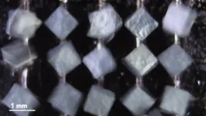
The technique takes advantage of a feature of a material called pyrolytic graphite, which can be levitated in magnetic fields above permanent magnets. SelfArry puts a layer of this material (which is, compared to graphene, is relatively easy to make) onto the LEDs then puts the LEDs, in volume, onto a chequerboard of permanent magnets that vibrates. The LEDs then jiggle into position between the different magnetic poles with, conveniently, just one at each position. There is a very short video online that shows the process – see the end of the article. After you have them all lined up, you just have to put the LEDs on the substrate. (see the videos at the end of the article)
SelfArray has a video showing 1mm Dies being distributed at 1.5mm centres
“Hmmm”, we said to Ballinger “Just?”.
“Ah yes”, he acknowledged, there may be something of a challenge there. After all, the LED chips may be stable in space, but need placing on the final surface still. If the chips are small enough, and at the moment, the target is chips around 100 ?m square so are quite light, even static charge may be enough to attract the aligned LEDs to a chuck and can then be transported to the final substrate. One of the purposes of the research fund is to investigate the best way of doing this.
Of course, the LEDs, once on the substrate, still have the carbon attached, which would cause a problem with transparency or conductivity, so “how do the ‘carriers’ come off?”, we asked. Ballinger said that the group had been worried about this, but the adhesives are not designed for long attachment (think PostIt Notes!) and the carbon can be peeled off or washed off with acetone. It turned out that this has not been an issue in development.
Dealing with omissions and defects should be, relatively, simple, SelfArray believes, using traditional machine vision and ‘pick and place’ technology to fill gaps. However, in its tests, the company has been getting very high levels of filling, which is helped by the fact that the LEDs can be, efffectively, poured over the magnetic area in large numbers, with those that don’t stick being sent around again. (This reminded me of the concept of ‘Fluidic Self Assembly’ developed and promoted by Alien Technologies for displays at SID in 1999 but which didn’t come to market in the end for displays, with Alien re-inventing itself around RFID chips)
Wouldn’t it be Nice?
The system has a key advantage that only occurred to me as I was writing up this article, so I didn’t discuss it with Ballinger.
Semiconductor processes produce a range of different performance and quality, so taking the LEDs directly from the wafer means that there can be little or no testing of the LED before it’s in place. That is going to mean some kind of quality checking process either on the wafer or on the substrate. If you do that you will have to eliminate some of the LEDs, some are bound to fall outside the acceptable range for efficiency or colour, even if they all worked (and with 25 million needed, that’s going to be very unlikely). That means you will have significantly undermined the value of the parallel process of placement.
On the other hand, the kind of process suggested by SelfArray would allow LEDs to be sorted and tested before placement as there is nothing special about how they are presented to the assembly process.
Heroes and Villains in Applications
SelfArray sees early applications in making LED modules for small pitch LED displays which are moving to Chip on Board (CoB) architectures. As you can see in the video, the company has used the technique on 1mm blocks and told us it has tried LEDs from 300?m down to 100?m and testing the limits will be part of the NSF research. They don’t see any reason in the physics why the LEDs couldn’t be very small, but there may be a catch in the engineering. As Ballinger said, the forces get smaller, but so does the weight of the LED.
Companies such as Absen and Silicon Core have shown this kind of technology at recent trade shows such as ISE. These LEDs could be small enough to benefit from the process and the typically small modules currently being used in CoB are ideal for an early development of the technology. The technology could also be very useful for smaller displays with miniLED backlighting – the kind of thing being developed for automotive applications.
The company is reasonably flexible on its long term business model, but doesn’t really want to be a machinery maker, so is looking to find partners for development and possible licensing.

