I think it’s one of those synchronicity moments. A few days ago, I put a note in my reminder box to follow up on a company that is working on joining LTPS substrates together in a seamless way. Today, The Elec reports that Samsung is looking to get supplies LTPS backplanes for microlEDs.

Tiling displays seamlessly is really, really difficult if you want those seams to be invisible. Some twenty years ago, a start-up called Rainbow Displays got some funding from Philips to tile small LCDs to get around some of the challenges of making big LCDs. Despite winning a “Display of the Year” award (it was a bit of a poisoned chalice at the time!), the firm went out of business in 2005 when the cost of bigger LCDs fell so far that they couldn’t compete.
One of the key problems is that the human eye is so sensitive to tiny changes in performance especially when they are in a line or pattern. For example, when LCD makers were in the early days of experimenting with very large LCDs, they couldn’t buy polariser film that was big enough to cover the whole display in a single sheet. In demos, it would be very obvious where the join was, despite the best efforts of panel makers.
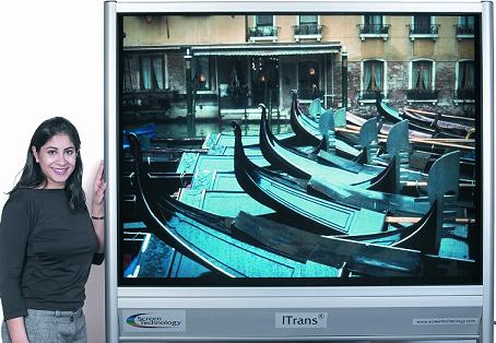 I did work with a start-up in the UK (Screen Technology) that developed a kind of pixel extension system based on plastic optical fibres that ‘flared out’ the pixels from standard LCDs to make a bigger image to hide the bezels and create a seamless tile concept. It was called iTrans and is shown in this image. Unfortunately, thermal expansion problems meant a need to leave small gaps (not visible here) and there was too much loss of contrast because of crosstalk between the pixels, so in the end, the concept didn’t make it to the mainstream although the firm did get some commercial orders. It closed in 2009.
Direct LEDs Are Tiled
Direct LED displays and particularly microLED technology has been based on the idea of tiling modules. In really big displays, with very bright LEDs, the seams can become invisible as there is so much contrast between the bright parts of the image and the tiles. Big LED walls need to be made with tiles (or cabinets) for logistical reasons. Big monolithic displays are an immense challenge. Panasonic had a production 100″ PDP that was a bit heavy and difficult and even made a small number of 150″ PDPs that were a nightmare to ship and install. The displays were nearly 2m along the shortest side, without any packaging, and were very very heavy. The longest side was over 3.3m – which meant that it wouldn’t go in most lifts, for example. I remember the grumbles from Panasonic marketing staff about the cost and hassle of moving units to events such as CES and IFA.
Anyway, early demonstrations by Samsung of direct LED TVs were based on larger modules that could be repositioned and even motorised – I remember a demo at CES of a display that reconfigured from a relatively square “4:3”-ish aspect ratio to a “16:9”-ish aspect ratio. That is very unlikely to produce a seamless look.
The best direct view microLED that I have seen is the Sony Crystal LED. That has amazing quality and the way that Sony demonstrated the video walls made the display look almost seamless. However, getting them to look that good needed a lot of on-site work by very patient technicians. The cost of that became a significant barrier to sales of the Crystal LED, so when the firm launched its most recent version (Sony Upgrades (and Downgrades) its Crystal LED), it emphasised changes that it had made to the mechanical design to make the alignment much more accurate, simpler and quicker to make the displays more accessible.
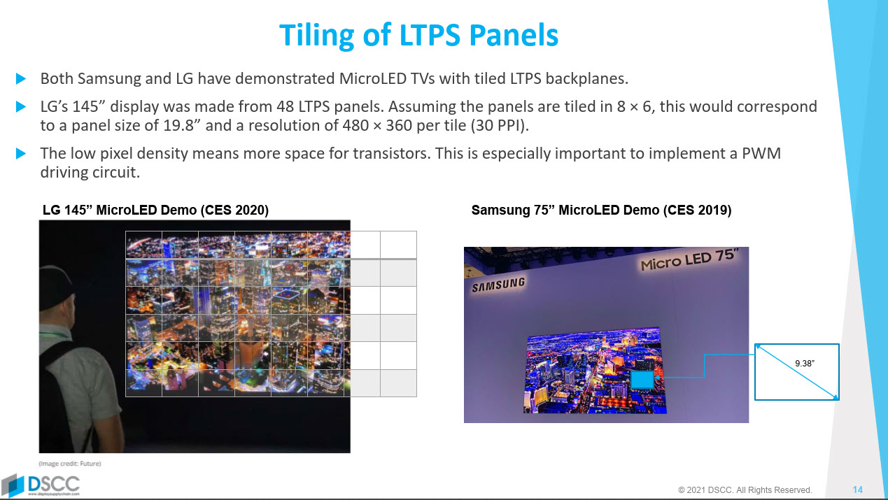
Samsung, LG and many others are looking at microLEDs in TV in sizes from somewhere around 75″ to 150″. Up to 100″, which has a longest edge of 2.2m, there is the possibility of shipping as monolithic units to homes, but above that, it pays to think about modular assemblies. There are two substrates that microLEDs of this type (so excluding microdisplays) can be mounted on – LTPS and PCBs. Both substrates have been shown by Samsung. Guillaume Chansin of DSCC said at the Display Week Business Conference that both LG & Samsung have made 145″ microLEDs using LTPS.
Chansin said that
“LG’s 145” display was made from 48 LTPS panels. Assuming the panels are tiled in 8 × 6, this would correspond to a panel size of 19.8” and a resolution of 480 × 360 per tile (30 PPI)”.
PCBs have the advantage of being cheaper to make than LTPS, while glass-based LTPS have the advantage of including active driving. Glass is also flat and avoids challenges such as distortion in the backplane. Ian Hendy wrote a Display Daily that dug into the complexity of microLED driving. (Driving the New Technology on the Block) and that highlighted that microLEDs will benefit a lot from more complex and sophisticated backplanes, whether based on LTPS, IGZO or other transistor technology.
Back at the missed Display Summit in 2018, Prof. Yong-Sang Kim gave a presentation on the different backplanes for microLEDs from microdisplays to large displays. That highlighted the point about the complexity of driving being a significant factor in a decision between PCBs and LTPS.
Samsung has developed its 110″ microLED that is said to use a PCB backplane, rather than LTPS although Samsung is widely reported to be keen on LTPS and the article in The Elec said that Samsung has approached AUO to potentially supply 12.7″ LTPS backplanes for this application. (AUO has shown LTPS-based microLED demos for several years) The Elec reports that such a substrate as costing $70 to $80 (and might cost even more if yield is poor) and you would need a lot to make a big TV (64 for a 101″ and 81 for a 114″). The paper also said that making LTPS backplanes for microLED requires 24 masks for production, compared to 11 to 12 masks for an OLED. That adds to the cost.
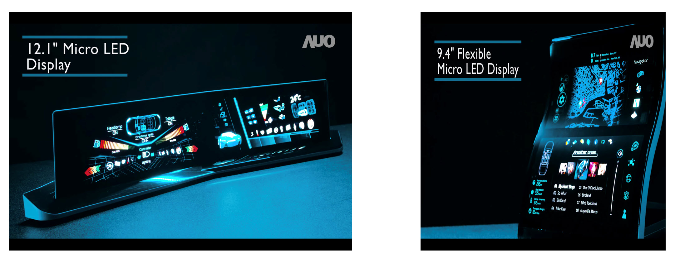 AUO has showed MicroLED displays based on LTPS
Separately, the ET News in Korea reported that a company called Laser Apps from Korea has reported that it has developed technology to cut and prepare the edges of microLEDs very accurately, to allow ‘side-wiring’ of microLED substrates. Using a laser is accurate to within 10 microns and avoids the edge damage of other processing techniques. (BR)