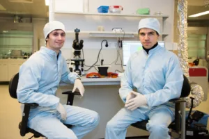
The team of scientists from the NUST MISIS Laboratory of Advanced Solar Energy engaged in the development of perovskite thin-film devices has proposed a new modification of the LED, for the first time using two-dimensional inorganic material, zirconium trisulfide, as the electron transport layer of the perovskite LED. In the future, this will allow starting mass production of a new type of light-emitting diodes, as well as solving the problem of LED displays degradation, for example, in smartphones and TVs.
An article on the development has been published in the Applied Materials & Interfaces journal.
The screens of many modern smartphones and TVs “suffer” from pixel burnout. Due to the presence of an organic component in OLED-type matrices (and their derivatives), pixels begin to degrade when the same icons on the screen are “highlighted” for a long time. So far, manufacturers advise users to periodically change the screen interface, rearrange the icons in places and regularly update the screen saver. In fact, the problem can be solved by minimizing the use of organic components in the screen matrix. Perovskite diodes are there to make a revolution in designing screens.
Perovskite materials are a young class of semiconductors that offers wide opportunities to reduce the cost of bright displays and some optoelectronic elements such as solar panels, lasers, photodetectors and light-emitting diodes (LEDs). The use of perovskites, in particular, for the production of LED screens for telephones or TV sets can significantly reduce the cost of production and extend their service life.
The scientific team of the NUST MISIS Laboratory of Advanced Solar Energy under the leadership of Ph.D. Dmitry Muratov has developed a perovskite LED in which two-dimensional zirconium trisulfide has been first used. For the first time, two-dimensional material is used as an alternative to the traditional organic layers of an LED device. In particular, the layer was formed with the use of the industrial method of slot matrix printing, which can help to quickly adapt the technology for mass production.
“At a certain stage of the research, the question inevitably arises: is the development suitable for implementation in mass production? The world experience in the assembly of perovskite LEDs is reduced to the layer-by-layer assembly of components by applying precursors to a rotating glass substrate. This allows us to achieve homogeneity of the layers, but it is completely unsuitable for mass production – this approach does not presuppose the simultaneous loading of several samples,” said one of the authors of the study, a research associate at the NUST MISIS Laboratory of Advanced Solar Energy Arthur Ishteev. “Therefore, we are interested in finding materials that would allow us to scale the production of perovskite LEDs.”
The scientists are working on the adaptation of perovskite application technology by analogy with the industrial methods of the semiconductor industry. This will eliminate the disadvantages of fading blue organic LEDs in modern displays by replacing them with stable perovskite diodes.

