A team of researches headed by Yong-Chun Ye of Soochow University (Suzhou, China) is developing an architecture for red light emitting perovskite based LEDs (PeLEDs) that “minimizes optical energy loss and significantly increases their efficiency and longevity.”

At this time, the commercial development of PeLEDs is hampered by insufficient long term operational stability. In fact, the typical period of continuous productive operation of PeLEDs has been limited to hours or even minutes.
Previous experimental work has identified the sources of optical energy loss in PeLEDs. One important cause of loss relates to the structures formed by the flat interfaces between layers within the device. More specifically, due to the reflection and partial parasitic re-absorption of internally confined photons by the layers of the LED. Such layers include the perovskite, hole transport, electron transport and glass layers. The significance of the optical losses and consequent decrease in light output is an increase in the amount of electrical power required to produce a given LED brightness. This, in turn, results in increased joule heating, an increase in device temperature and a decreased in device lifetime.
The approach adopted by the team to address these issues was based on modifying the light emitting nanostructures within the PeLED.
A recent article by the team on this topic is entitled “Minimizing Optical Energy Losses for Long-Lifetime Perovskite Light-Emitting Diodes.” It was published in Adv. Funct. Mater. 2021, 2105813. A copy of the article is available for purchase and can be found here.
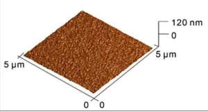
In the team’s new approach, the surface of the LED substrate was “complicated by a certain order of numerous ‘patterns’ – ‘hemispheres’ several nanometers high.” The surface structure of a representative conventional flat and an experimental patterned substrate are illustrated in the figure below.
 Film morphology of representative flat and patterned substrates. Atomic Force Microscope images of (left) a conventional flat PEDOT:PSS film on ITO glass and (right) of an experimental, patterned PEDOT:PSS film on ITO glass.
In the figure, PEDOT:PSS refers to an acronym for poly(3,4-ethylenedioxythiophene) polystyrene sulfonate, a transparent, conductive polymer that has high ductility.
The patterning was found to lead to a significant reduction in the re-absorption of photons. With an increase in light output, the amount of electrical power required to produce a given LED brightness was also reduced and, consequentially, the joule heating decreased.
Some top level details of the results reported in the article are as follows:
- By comparison: in a LED with a flat substrate, the surface temperature rose to 32°C in 20 seconds. In 50 seconds, it rose to 35°C. In an equivalent device with a patterned substrate, the surface temperature rose to 30°C in 100 seconds and then stabilized at this level. Reducing the temperature of the LED prevented thermal degradation and prolonged device lifetime.
- The peak quantum efficiency of a LED device with a patterned substrate was 21.2%, twice as high as that of an equivalent LED with a flat substrate. Given the same power input, a LED with a patterned substrate was about 2.5 times brighter and its period of productive operation was 1.75 times longer.
- At a wavelength of 666 nanometers and an initial luminosity of 100 candle/square meter, the resulting peak quantum efficiency of the LED with a patterned substrate was maintained for nearly 4807 hours. The researchers stated that “This is the longest high performance lifetime compared to similar PeLEDs available in the world.”
The team concludes their article with the statement that “The enhanced light extraction from trapped modes can efficiently reduce the driving current and suppress optical energy losses in PeLEDs, which in turn ameliorate the heat-induced device degradation during operation. This work paves the way toward high-performance PeLEDs for display and lighting applications in the future. -Arthur Berman
East China Normal University, Yan-Qing Li, [email protected]

