Metal halide perovskites have several optoelectronic properties that make them attractive for use in a wide variety of device applications. The successful use of such materials in some desired applications has, however, presented a challenge. The reason is that many optoelectronic devices require the production of arrays having a layer of single crystal perovskite and that the layer has excellent chemical stability, low defect density, and high carrier mobility. There is, therefore, a need to develop means for precise control of on-chip fabrication of large-scale perovskite single crystal arrays. Addressing this issue was the subject of a recent study by a team of researchers led by Zhangsheng Xu of the School of Nanoscience and Technology, University of Chinese Academy of Sciences (Beijing, China).
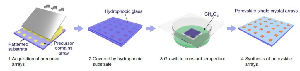
The approach adopted by the team to achieve homogeneous perovskite single crystal arrays is a one-step process described as “Space Confinement and Antisolvent Assisted Crystallization” or SC-ASC.
A recent article on this topic by the team is entitled “Controlled on-chip fabrication of large-scale perovskite single crystal arrays for high-performance laser and photodetector integration.” It was published in Light: Science & Applications (2023) 12:67. A copy of the article can be downloaded here.
As described in this article, the keys to realizing fully controlled growth are:
- Substrate engineering to ensure accurate pixel positioning.
- Space confinement to regulate the extraction of contact line without leaving residue.
- Antisolvent crystallization to improve the crystal quality.
The figure below illustrates the process developed by the team to synthesize a perovskite so-called microplate array.
Some of the more important details of this approach are as follows.
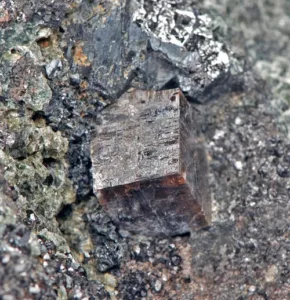
The process fabricates high-quality single crystalline MAPbBrxCl₃-x (MA = CH₃NH₃, x = 0, 1, 2, 3) microplate arrays. Fabrication on various substrates was possible, in part, due to the fact that the SC-ASC method is a low-temperature procedure.
The team demonstrated that the SC-ASC approach was capable of enabling precise control of crystal arrays spanning an area of 100 cm². In addition, the approach enabled different array shapes and resolutions with less than 10% pixel position variation, tunable pixel dimensions from 2 μm to 8 μm as well as the in-plane rotation of each pixel.
Based on the ability to fabricate a perovskite array aligned on patterned electrodes, the team demonstrated an independently addressable photodetector array with a vertical structure. This array was capable of imaging input patterns.
The researchers concluded their article with the statement that “The concept of this strategy is universal and we expect that it can be expanded to fabricate other solution processed semiconductors.”