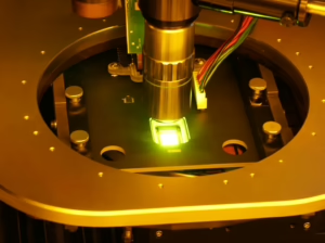
As augmented reality (AR) devices rapidly evolve, display requirements become more demanding. AR eyewear must deliver clear, high-contrast images in brightly lit environments, all within a tight power budget. Researchers at the Fraunhofer Institute for Photonic Microsystems IPMS have addressed these challenges by developing a novel multiple stacked OLED architecture. This design not only delivers extraordinary luminance levels—above 70,000 Nits for a monochrome microdisplay and over 200,000 Nits on reference substrates—but also provides a pathway to lower power consumption and longer device lifetimes.
Unlike conventional desktop or television displays, AR microdisplays are used in devices that project or guide the emitted light through waveguides, holographic elements, or additional optics. Each optical component along the path can reduce the intensity of the light that reaches the user’s eye. As a result, initial luminance must be extremely high to remain clearly visible, especially outdoors.
In parallel, miniaturized wearable devices (e.g., AR glasses or headsets) are often powered by batteries that cannot supply large currents for extended periods. This creates a fundamental design challenge: how to boost brightness without dramatically raising power consumption or compromising the display’s operational lifetime.
The researchers at Fraunhofer IPMS have demonstrated that stacking individual OLED units can resolve many of these issues. In a tandem OLED configuration, the OLED layers are arranged in series, each layer emits light when the same current flows through the stack. Brightness effectively increases with each additional layer because the total emission is the sum of the emissions from all active layers. Critically, the current density within each individual layer can be kept the same as that of a single-layer design, thus reducing the overall stress on each emissive unit.
This principle enables researchers to achieve very high luminance at moderate current densities, paving the way for prolonged device lifetime, since lower current density typically leads to slower degradation snf flexible operating conditions, allowing displays to be driven at extreme brightness when needed (e.g., under direct sunlight) or at lower brightness for efficiency.
Quantitative data from the Fraunhofer IPMS team highlights the tangible gains of stacked OLEDs: such as a marked increase in operational lifetime: for instance, at 50,000 Nits, shifting from a 1-unit to a 2-unit design improved the LT95 (time for brightness to drop by 5%) from 900 to 1300 hours.
High-resolution microdisplays typically feature pixel pitches on the order of micrometers. In some AR applications, they can be even smaller to accommodate greater pixel densities for sharper images. When OLED thickness increases—such as in tandem structures—the risk of optical crosstalk (light leaking from one pixel to adjacent pixels) rises.
Fraunhofer IPMS researchers are investigating innovative optical isolation approaches (e.g., protective barriers, microstructuring, advanced planarization techniques) to mitigate this pixel-to-pixel interference. Solving the crosstalk challenge is key for maintaining the microdisplay’s high contrast and color fidelity.
An additional advantage of stacking multiple OLED units is the potential for narrowband emission at high brightness. Narrowband emission can significantly reduce undesired spectral components, which is beneficial for waveguide coupling (improving efficiency) or for holographic elements that rely on precise wavelengths. By precisely tuning the organic materials, researchers can optimize the overall emission spectrum to suit particular AR optical architectures.
By tackling these challenges, multiple stacked OLED technology can solidify its role in the competitive AR market. The Fraunhofer IPMS is actively seeking collaborators and commercial partners worldwide to translate laboratory-level achievements into market-ready solutions.

