Our good friend, Dr. Jon Peddie, got to hear about the next generation Snapdragon 820, launched today. Very high resolution displays and graphics need significant processor power to drive them and this is where Qualcomm’s DSPs come into play.

Qualcomm has been the leader in building truly heterogeneous SoCs, which include a 64-bit CPU, a powerful GPU, dual ISPs, and a few DSPs, which Qualcomm brands as Hexagon. Other SoC builders have DSPs in their chip, but use them primarily for audio or modem functions. Qualcomm does that too but also dedicates one to video and image processing.
What’s new in the Snapdragon 820 is the extended Hexagon DSP, which Qualcomm has designated the 680. The company is employing the signal processing capabilities of the 680 with the two Spectra ISPs in the Snapdragon, which makes for a powerful, and very fast image processing system— the processing power that filled a 2U rack 10 years ago, now fits in your pocket.
Because a DSP is such a special device it can process the 16 bit fixed image data much faster than a conventional CISC FP processor, with the same accuracy. And it can do it with less power. For imaging, for example, the DSP can generate results ~3x faster at ~10x lower energy (vs. quad-CPU).
It is important to remember that this wide vector capability is an extension to the core. That is, the core retains all the previous capabilities, concurrently supporting SIMD 64-bit for 8/16/32 bit fixed point as well as 32-bit floating point. The DSP’s special ISA offers sliding window filters, LUTs, histograms, and performance sufficient for UHD video, or post-processing of 20Mpix camera burst mode processing … and more.
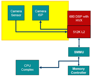
The 680 takes data from the SoC’s ISP via a L2 cache, and returns image processing and filtering results the system memory and CPU, as illustrated in the following block diagram.
 Qualcomm’s use of the Hexagon 680 DSP as the streaming pre-processor for image processing (Source Qualcomm)
So what?
So with a wide-word signal processor in the front end, image things can be run really fast. With ever increasing sensor resolution, and higher resolution screens, you need to move pixels from the front end to the screen fast, and they need to look right when they get there.
Qualcomm compared the DSP with HVX vs. just a Quad Krait CPU with full Neon-Optimization. The Quad Krait CPU was run at 2.65GHz, and the single DSP/HVX ran at 725MHz. The results are shown in the next diagram.
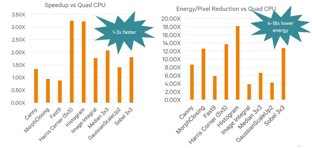 Typical image tests show the benefit of combining the DSP with the ISP, as compared to just using a CPU (Source Qualcomm)
The point Qualcomm is trying to demonstrate here is that for the super smart phones that will be coming out in 2016, with mega sensors and big high-res screens, you need more image processing horsepower than you can get from just a CPU, no matter how many cores you jam into that CPU.
Qualcomm actually puts three DSPs in its SOC.
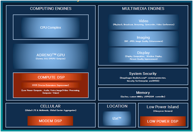 The Snapdragon 820 has a big computer DSP for image processing and other workloads, a traditional modem DSP, and low and separately powered DSP for always on listening (Source Qualcomm)
The low-power island DSP is for “always on” sensor processing. This is a major breakthrough for Qualcomm, and the industry. Putting the sensor hub inside the SoC saves board space, and most importantly power. The chip has a new power management schema to be “always off” until needed. That gives a longer battery life for key use cases (e.g., pedometer or sensor-assisted positioning).
Qualcomm is claiming to be the first in the SoC market with super wide vector SIMD extensions for their DSP. And they claim it can be exploited through conventional tools and techniques, using shared memory POSIX-like threads (on DSP RTOS), and a LLVM compiler. This, says the company, allows programing with C/C++ and Intrinsics, and a suite of pre-optimized libraries for common filters & algorithms.
What’s not to like? – Jon Peddie
(Jon’s own Jon Peddie’s Techwatch will contain more geeky details on the architecture)