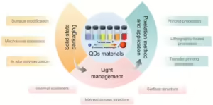
A review by researchers at the Karlsruhe Institute of Technology (KIT) in Germany takes a look at the advantages of quantum dots (QDs), such as their high photoluminescence quantum yield (PLQY), small particle size, and solution processability, and their suitability for color conversion in Mini/MicroLEDs. It’s an interesting paper that covers all the types of QDs, including Cd-based QDs, InP-based QDs, and perovskite QDs, comparing their emission properties, PLQY, and stability.
The researchers identify several challenges, such as the stability of QD materials, dispersion quality in solid-state matrices, light extraction efficiency, and the precision of mass manufacturing processes for QD pixelation and addresses issues like the high toxicity of Cd-based QDs and the relatively lower performance of InP-based QDs.
The paper discusses approaches to improve light management in QD composites, such as the introduction of internal scatterers, internal porous structures, and surface structures to enhance optical outcoupling and photoluminescence intensity.
These methods help reduce QD light reabsorption and improving the overall efficiency of the color conversion layers.
High-precision fabrication methods for RGB QD pixel arrays are crucial for achieving high-resolution displays. The review outlines the current research on QD pixelation techniques and their potential for industrialization.
Pixelation issues in the context of QD-based Mini/MicroLED displays refer to the challenges associated with precisely placing and controlling QDs at the micro-scale to form high-resolution, full-color displays. These issues are critical because the performance of QD-based displays depends on the accurate positioning and size of QD pixels, which directly impact the color quality, brightness, and overall display resolution.
MicroLED displays require extremely high resolution, often with pixel sizes smaller than 100 µm. Achieving this level of resolution necessitates precise control over the deposition and patterning of QDs, which is challenging with current manufacturing technologies. For a display to produce uniform color and brightness across the screen, the QDs must be uniformly distributed and precisely aligned with the underlying LED pixels. Any misalignment or variation in QD distribution can lead to color inaccuracies, brightness inconsistencies, and reduced display quality.
The researchers highlight the lack of high-precision mass manufacturing techniques for QD pixelation. Current methods often lack the fine control needed to consistently produce high-resolution QD patterns at scale. This is a significant barrier to the widespread adoption of QD-based MicroLED displays in consumer electronics.
The interaction between QDs and the substrates they are deposited on plays a crucial role in pixelation. Issues such as poor adhesion, differential thermal expansion, and chemical incompatibility can lead to defects in the QD pixels, further complicating the pixelation process. When QDs are deposited onto a substrate, their tendency to spread or contract due to surface tension can affect the final pixel size and shape. Controlling this behavior is crucial for achieving consistent pixel sizes, especially at the micro-scale.
| Method | Feature Size | QD Material | Color of Emission |
| Aerosol Jet Printing | 30 µm (line width) | CdS, CdSe/ZnS | RGB |
| Inkjet Printing | 200 µm × 75 µm (pixel size) | CsPbBr3 | Green |
| Inkjet Printing | 110 µm (pixel size) | MAPbBr3 | Green |
| Electrohydrodynamic Printing | 3.9 µm (dot size) / ≈400 nm (line width) | CdSe/CdZnSeS, CdSe/CdS/ZnS | Red, green |
| Electrohydrodynamic Printing | 1 µm (dot size) | CdSe/CdS/ZnS | Red |
| Electrohydrodynamic Printing | ≈890 nm (line width) | CdSe | RGB |
| Photolithography | 10 µm (pixel size) | – | Red, green |
| Projection Lithography | 21 µm (pixel size) | CdSe/ZnS | Red, green |
| Indirect Photolithography | 5 µm (line width) | II–VI core–shell QDs | RGB |
| Indirect Photolithography | 8 µm × 40 µm (pixel size) | CdSe/ZnS | RGB |
| E-beam Lithography | ≈30 nm (line width) | CdSe/CdS | Red |
| X-ray Lithography | 150 µm (pixel size) | CsPbI3, CsPbBr3 | Red, green |
| Laser Direct Writing | ≈170 nm (line width) | CdTe | Green |
| Laser Direct Writing | 900 nm (line width) | CsPbI3 | Red |
| Laser Direct Writing | 3.3 µm (line width) | CsPbBr3 | Red |
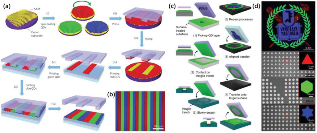
| Transfer Printing | 400 nm (line width) | CdSe/CdS/ZnS, CdSeS, CdS | RGB |
| Transfer Printing | 6 µm (pixel size) | CdSe/ZnS, CuInSe, PbS | RGB |
Poor pixelation can lead to color mixing, where adjacent pixels bleed into each other, reducing color purity and accuracy. This is particularly problematic in high-resolution displays where pixels are closely packed. Inconsistent QD placement can also affect the brightness and efficiency of the display. Areas with higher concentrations of QDs may appear brighter, leading to an uneven display, while poorly distributed QDs can reduce overall light conversion efficiency.
The paper suggests that future research should focus on developing advanced fabrication techniques that can achieve the necessary precision for QD pixelation while being scalable and cost-effective. Techniques such as advanced photolithography, laser-assisted deposition, and self-assembly of QDs are potential areas of exploration. Enhancing the compatibility between QDs and substrates through surface modification or the development of new materials could also help address some of the pixelation challenges, according to the researchers
Reference
Chen, J., Zhao, Q., Yu, B., & Lemmer, U. (2024). A Review on Quantum Dot-Based Color Conversion Layers for Mini/Micro-LED Displays: Packaging, Light Management, and Pixelation. Advanced Optical Materials, 12(2), 2300873. https://doi.org/10.1002/adom.202300873