MakerBot announced another 20% workforce reduction last week. Despite a cult-like following among the DYI crowd (digital do-it-yourselfers), the 3D printer maker seems to be having trouble realizing the business plan it inked. This doesn’t surprise me; the real money is in inks, not in the tools. Specialty chemical firms tend to become enabling links in supply chains that create new-to-the-world products. Once a printer maker learns how to turn dots into films, continued innovations often come from the proprietary inks that engineers can put into a printer tool and onto a substrate.
![]()
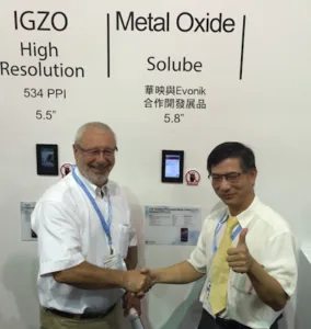
For this reason, I was happy to read a press release on the same day announcing results from a metal-oxide ink for TFT channels supplied by Evonik and used by Chungwha Picture Tubes (CPT). Evonik has been characterizing and improving its line of iXsenic inks for several years, so a practical demonstration was no surprise. What I found surprising is that CPT was able to make an LCD smartphone panel with it. I had assumed early applications would target simpler things such as sensor circuits.
My experience with coating/printing materials such as dielectric or light shield films suggests that some panel makers are afraid of introducing organic inks into production environments. They may worry about ink stability and reproducibility: storage, self-life and handling. They may anticipate problems with material interactions between adjacent films or with thermal budgets (it may be best to start with the highest process temperature, then reduce it on each subsequent layer). I guess CPT moved beyond such concerns.
After all, there is a lot to like. Besides lower process temperatures and costs, coating metal-oxide channel films sure seems a lot easier than trying to deposit microcrystalline or other high-mobility films in vacuum. You may recall that initial research into metal-oxide TFT such as IGZO explored methods of forming micro-crystalline or poly-crystalline channels. More recently, we read about development of c-axis-aligned (micro) crystalline IGZO TFT at Semiconductor Energy Laboratory. As I expected, practical applications remain elusive because amorphous films are so much easier to achieve in production.
After all, if electron mobility was so important, we would have seen many more polysilicon (i.e. LTPS) fabs pop up since 2000. A number of polysilicon fabs are ramping up to serve the advanced smartphone market now, but most of the industry’s expansion remains amorphous-silicon based because a-Si is good enough. Thus, the time of chasing mu (? is a symbol for electron mobility) may be ending… I hope so. I am tired of hearing the song “My mu is bigger than you mu” sung at every conference. Stable n-channel metal oxide devices with mu near 10 will be good enough for a lot of practical devices, be they 8K TV panels or wearables. The hare doesn’t always beat the tortoise in a race to production.
Evonik and CPT at Touch Taiwan
The fact that CPT chose to be a lead user of coatable semiconductors is also promising. I recall that CPT was a lead user for DuPont’s ill-fated thermal-transfer color filter system but that project failed partly because the industry was shifting into chevron-shaped (e.g. MVA or IPS) pixels and the first Gen-8 fabs were coming on-line. CPT may be a better development partner today because it is interested in the broader field of optronics. There is a lot of room for product innovation beyond yet another mobile display… some of the system-level designs shown by Thinfilm come to mind in this regard. Optronic product ideas may even foster display innovations after reaching scale in less competitive markets. In any case, no one seems to be making a lot of money by investing in displays, alone.
So inks may show us a different future than one toward which industrial momentum is taking us by default. Building another Gen-too-big fab to make another jillion panels will not foster innovation. Isn’t it time to start printing money? (DB)