
A collaborative research team from Korea and the UK, led by researchers from Pusan National University, has significantly improved signal amplification in CsPbBr3 perovskite nanosheets. Perovskite nanosheets are two-dimensional materials, part of the broader category of perovskite compounds known for their distinctive cubic lattice crystal structure. These nanosheets, characterized by their thin, sheet-like formation at the nanoscale, exhibit unique electronic, optical, and photovoltaic properties. The high surface area and quantum properties of these nanomaterials make them suitable for a variety of applications across different fields.
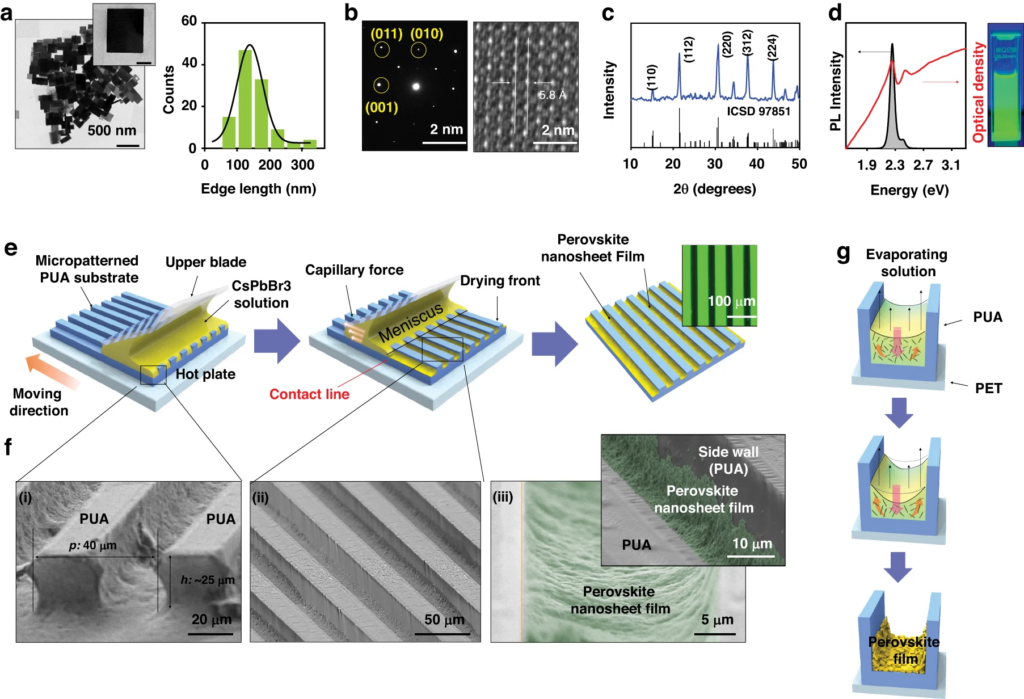
b. This part displays the Selected Area Electron Diffraction (SAED) pattern and a high-resolution TEM (HRTEM) image of the nanosheets, demonstrating their crystalline structure.
c. An X-ray Diffraction (XRD) pattern of the CsPbBr3 nanosheets is shown, with a comparison to the standard XRD pattern for the orthorhombic phase, indicating the crystal structure of the material.
d. This section features the absorption (optical density) and photoluminescence (PL) spectra of a colloidal solution of the nanosheets that emit green light, showcasing their optical properties.
e. Illustrates the process of depositing CsPbBr3 nanosheets onto a patterned polyurethane-acrylate (PUA) substrate. An inset shows an array of green fluorescent images of the resulting perovskite film.
f. A series of Scanning Electron Microscopy (SEM) images provide different perspectives of the CsPbBr3 nanosheets deposited on the patterned PUA substrate. It includes a front view, a tilted side view, and a magnified top view of the sidewall of a single waveguide channel.
g. Finally, a schematic diagram details the sequential deposition processes used to apply the nanosheets onto a single microchannel. (Source: Light: Science & Applications)
The team introduced a new method of gain analysis termed gain contour, which surpasses previous techniques in assessing light amplification capabilities. Unlike older methods that provided only a gain spectrum, gain contour analysis illustrates how gain varies with spectrum energy and optical stripe length, offering a more comprehensive understanding of local gain variations.
Further examination revealed that the perovskite nanosheets’ excitation and temperature dependence, combined with a patterned waveguide made from polyurethane-acrylate, substantially improved gain and thermal stability. These advancements were attributed to better optical confinement and heat dissipation, facilitated by two-dimensional center-of-mass confined excitons and localized states due to inhomogeneous sheet thickness and defect states.
This breakthrough not only paves the way for more efficient and controlled signal amplification in perovskite nanosheets but also holds promise for the development of more reliable and versatile optoelectronic devices. Potential applications include lasers, sensors, solar cells, encryption and decryption technologies, neuromorphic computing, and visible light communication.
Moreover, the enhanced amplification and efficiency could help perovskite solar cells become more competitive against traditional silicon-based alternatives. In the broader scope of optics and photonics, these findings could optimize laser operations, improve signal transmission in optical communications, and boost sensitivity in photodetectors, leading to more reliable device operations.
The long-term implications are vast. When intense light is needed at the nanoscale, these nanosheets could be combined with other nanostructures to serve as optical probes. The research team suggests that while perovskite quantum dots have been explored for lasers, their zero-dimensional structures have inherent limitations. The two-dimensional structure of perovskite nanosheets presents a promising alternative, potentially revolutionizing the field of optoelectronics.
In the realm of display technology, perovskites, including their nanosheet form, have shown great potential due to their exceptional light-emitting capabilities. They are particularly noted for their ability to produce bright, vibrant colors across a broad spectrum, making them a valuable candidate for next-generation light-emitting diodes (LEDs). Perovskite-based LEDs (PeLEDs) are being researched for their potential in producing high-quality displays with advantages like lower production costs and enhanced color saturation.
However, the commercial use of perovskite nanosheets in display technology is still in the developmental stage. There are ongoing challenges, such as ensuring stability, scalability, and mitigating toxicity issues, that need to be addressed. Despite these challenges, the research and advancements in utilizing perovskite nanosheets in display technologies are progressing, indicating a promising future for their application in electronic displays and other related technologies.
Reference
Kim, I., Choi, G.E., Mei, M. et al. Gain enhancement of perovskite nanosheets by a patterned waveguide: excitation and temperature dependence of gain saturation. Light Sci Appl 12, 285 (2023). https://doi.org/10.1038/s41377-023-01313-0