High dynamic range (HDR) is a hot topic in the display industry right now, with Dolby and many others working on the issues involved. Currently, the highest dynamic range CMOS camera sensor designs can capture up to 22 stops of dynamic range, just barely enough for “high dynamic range.” And most camera sensors are much lower than this, more in the range of 12 – 14 stops.
Capturing even 22 stops really is only just barely enough for HDR because it provides no overhead for video editors to adjust the exposure. HDR cinema or TV may cover, well, a high dynamic range but the range is no match for the very, very, high dynamic range that would be needed to realistically capture everything in nature. Editors want to adjust the highlights in the video to the 1000 – 4000 nits maximum in a HDR display and keep the average brightness down to reasonable levels for a variety of reasons, such as eye comfort and display power consumption.
Panasonic gave three papers at the recent ISSCC 2016 (International Solid-State Circuit Conference) which was held in San Francisco from January 31 to February 4. These papers discussed camera sensors using an organic photoconductive film (OPF) they have developed in collaboration with Fujifilm. Panasonic said the OPF material could greatly increase both the dynamic range of cameras and the ability of the cameras to capture fast motion without artifacts.
The three papers were titled:
- An Over 120dB Simultaneous-Capture Wide-Dynamic-Range 1.6e- Ultra-Low-Reset-Noise Organic-Photoconductive-Film CMOS Image Sensor by K. Nishimura, et. al.
- 210ke- Saturation Signal 3?m-Pixel Variable-Sensitivity Global-Shutter Organic Photoconductive Image Sensor for Motion Capture by S. Shishido et. al.
- 1280×720 Single-Photon-Detecting Image Sensor with 100dB Dynamic Range Using a Sensitivity-Boosting Technique by M. Mori et. al.
 Comparison of a conventional CMOS sensor with a OPF CMOS Sensor
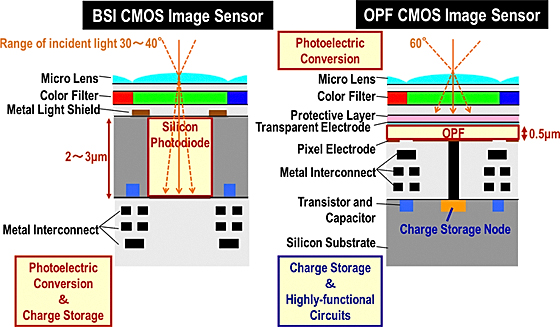
The difference between a conventional CMOS sensor and the new CMOS sensor with OPF technology is shown in the above figure. In the conventional sensor on the left, the silicon photodiode serves two functions. First, it converts incoming photons to electrons. Second, it stores these electrons until the end of the frame time where they are downloaded via the shown metal interconnects to the ADC and converted to a digital light level. The fact that the silicon photodiode serves two very different functions means it can’t really be optimized for either function without, at least potentially, degrading the other function.
In the right hand side of the figure, an OPF CMOS image sensor is shown. This design separates the two functions. The organic photoconductive film (OPF) developed by Fujifilm converts the incoming light into electrons. These electrons are then collected in the silicon charge storage node, developed by Panasonic. Since the two functions are separate, they each can be optimized independently of the other. The charge storage node, since it can be optimized for charge storage, can store about 10x more charge than the CMOS silicon photodiode before it saturates, increasing the brightness of the highlights it can capture.
The OPF design provides some bonus features, compared to the pure CMOS design. First, the OPF film can be continuous, providing a much larger aperture ratio than the limited size that the silicon photodiode provides. Second, because it is very thin, the OPF layer can accept a much wider angle of incoming light, allowing the use of lower f/# lenses. Both of these bonus features increase the sensitivity of the sensor in low light levels.
High Dynamic Range Captured by the new OPF CMOS sensor
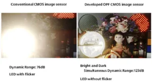
This figure shows a HDR image captured by the new sensor compared to the same image captured by a conventional camera. The HDR image was compressed in dynamic range by Panasonic to allow it to be shown on conventional displays, such as the one you are looking at. If you look at the LED array in the upper right corner of each image, you can see that the CMOS camera only captured part of the array because of the flickering nature of LEDs. The OPF CMOS sensor captured the entire array.
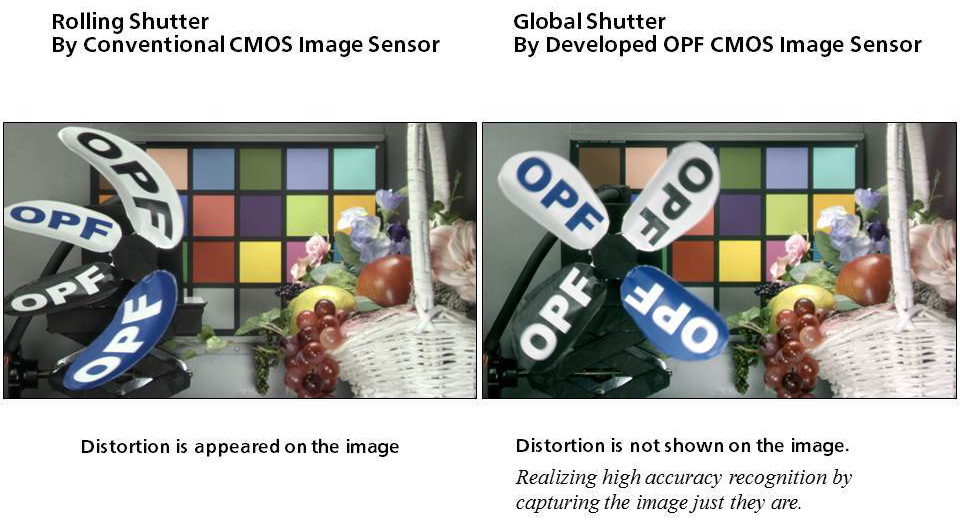
Wait! We’re not done! That is to say, Panasonic has another benefit the OPF CMOS sensor can provide. In the top figure you see a layer called “Transparent Electrode.” By varying the voltage on this layer, Panasonic can vary the sensitivity of the OPF layer, i.e. they can turn the pixel on and off. In fact, they can turn all the pixels on and off simultaneously, i.e. this is a global shutter. When you are trying to capture fast motion, a global shutter is essential to avoid motion artifacts, as shown in the image below. So a camera made from a OPS CMOS sensor is not only good for HDR, it will be good for high frame rate (HFR) use as well.
 No distortion is shown in the fast moving fan blades because of the OPS CMOS global shutter
The third paper Panasonic presented at ISSCC describes a 1280 x 720 image capture sensor developed by Panasonic containing the OPF CMOS technology. Presumably, this prototype sensor was used to capture the images for HDR and the global shutter.
This is not an entirely new technology – it was first announced by Panasonic and Fujifilm in 2013. Now that they have a sensor with the technology in it, it wouldn’t surprise me if they demonstrated a camera containing the technology at the upcoming NAB in Las Vegas, April 16 – 21, 2016. Will they also announce the commercial availability of a camera? We’ll have to wait and see. It’s a long development road from camera sensor to camera, from ISSCC to NAB and SMPTE. –Matthew Brennesholtz
For the press release plus a deeper discussion of the OPF CMOS technology, go to http://news.panasonic.com/press/news/data/2016/02/en160203-5/en160203-5.html
For the press release plus a deeper discussion of the global shutter technology, go to http://news.panasonic.com/press/news/data/2016/02/en160203-6/en160203-6.html

