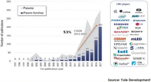
MicroLEDs were a very popular topic at the QLED & Advanced Display Summit (ADS), with eight talks taking up most of the second day of the conference. One reason the topic was popular at the ADS was that it is an extremely popular topic in the display R&D community, as shown by the rapid growth of patents published on the subject, as shown in the figure.
Patents related to microLEDs published by year, 1997 – 2017. (Credit: Yan at ADS, data originally from Yole Development)
Even display experts working in the microLED field like Ken Werner writing for Meko find the rapid advancement of microLED displays and the very high image quality they can produce surprising. Since the topic of microLEDs was such a new and unfamiliar topic to most of the ADS audience, each speaker felt obligated to give an introduction to microLEDs as part of his talk. Rather than go sequentially through the speakers, I will first cherry-pick this introductory material from all the speakers and collect it into a general microLED introduction. Following that, I will then give details from the individual talks, many of which discussed the details of the microLED display manufacturing process.
 LED size ranges for displays (Credit: Prof. Yan at ADS)
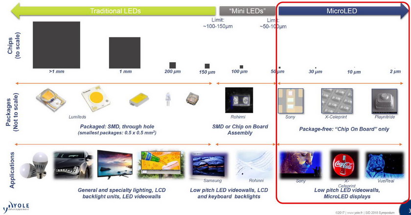 Applications for various LED size ranges. (Source: François Henley at ADS. Original image from Yole Development)
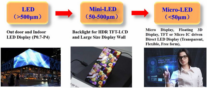
First, a note on the terminology: Professor Qun (Frank) Yan from Fuzhou University and General Manager of SID China gave the first talk on microLEDs and defined them as being smaller than 50µm on a side, as shown in the image. This same 50µm cutoff limit was used by Yole Development at SID 2018 and was cited by Francois Henley from Tesoro Scientific and QMAT Inc in his talk.
This cutoff point was debated during the panel session following the talks and many felt this was too small and 100µm was a more appropriate cut-off point between miniLEDs and microLEDs. It was generally felt by ADS attendees that LED die smaller than 100µm can no longer be handled by conventional LED and miniLED processing techniques and new manufacturing techniques are needed.
Since Bob Raikes at Meko had already asked his contributors to use 100µm as the cutoff between mini and microLEDs, I will continue to use that limit. BTW, the Meko consensus is that one day we will need to define a Nano or PicoLED limit, but not today, and the subject did not come up at the ADS. The smallest LED die discussed at the ADS were 3µm on a side. When microLEDs get too much smaller than 3µm, quantum mechanical effects must be taken into account and suddenly you have electroluminescent Quantum Dots, not LEDs.
Advantages and disadvantages of microLED displays
The eight speakers universally agreed that if you ignored cost, LED, miniLED and microLED displays were the best displays in all display sizes from smartwatches to giant cinema screens. There was no discussion of very large LED displays for digital signage at the ADS, but they appear to be the best for that market, too, since they currently totally dominate that market. There was also no discussion of miniLEDs at the ADS, except for their use in LCD backlights, especially for multi-zone dimming applications for HDR LCD systems.
Universally acknowledged advantages of LED displays included:
- Large color gamut (≥DCI P3).
- High brightness and very low black levels leading to a very high dynamic range and contrast.
- High contrast even with ambient light – small microLEDs with typical display pitches can have up to 99% of their surface covered with black absorbing material (e.g. Sony Crystal LED).
- Small microLED size on transparent substrates allow very high transmission transparent displays.
- The large empty areas between microLEDs in a display can be used for other functions such as sensors.
- Fast – can be addressed at arbitrarily high frame rates, depending on the backplane.
- Wide viewing angles (like OLED).
- Curved and flexible backplanes are possible (like OLED).
- Most energy efficient display technology – up to 220lm/W for white LEDs or 92 lm/W for green.
- Long life which may exceed 50K hours.
- No image retention or burn-in.
- High pixel density – up to 6000ppi (VueReal)
- Other functions including visible light communication with high data rate and multiple channels, position localization, etc. can either be built into the display or used as non-display stand-alone systems.
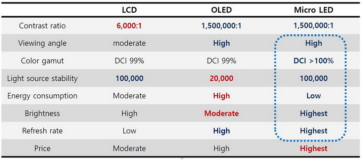 Key advantages of microLED displays compared to LCD and OLED displays. (Source: Jihoon Kang at ADS)
The advantages of microLED displays compared to LCD and OLED display were summarized in the table shown above from Samsung. Unfortunately, while microLED displays have the best image quality, it is never possible to ignore display cost. In addition to very high cost today, microLED displays have a few additional disadvantages:
- Cost, which breaks down into three major factors:
- Material cost of the LEDs (Epi cost)
- Assembly cost of putting the LEDs on the backplane
- Yield, which includes both Epi and assembly yield.
- LED color and efficiency vary with drive level
- LED color and efficiency vary with temperature
- LED color and efficiency may vary with die size
- Current-driven LEDs require more complex pixel circuitry than voltage-driven LCDs.
- Assembly techniques are completely different from previous display and non-display technologies
- Very large number of microLED die requires very high transfer rates
- Did I mention the very, very high cost of microLED displays?
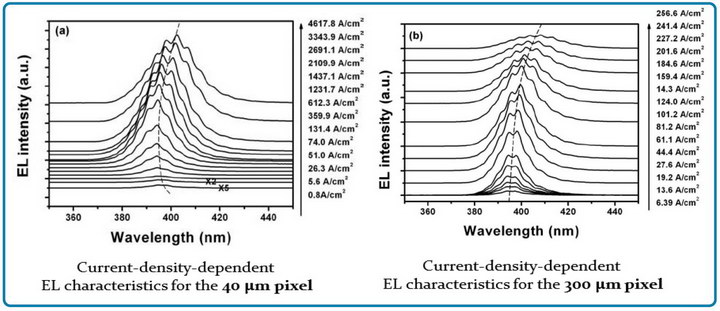 Wavelength shift data from drive level changes for a deep-blue GaN LED (Source: Prof. Yong Sang Kim from SungKyunKwan Univ.at ADS)
The color and efficiency problems are well known LED problems that also have well known solutions. These problems can vary by die size, as shown in the figure. The solutions to these problems, which were developed for displays with larger LEDs than microLEDs, need additional development to make them usable for smaller die. Both OLED and microLEDs are current driven so much of what has been learned about driving OLEDs will apply to microLEDs. To solve the color and efficiency with drive issue it is (probably) necessary to drive the microLEDs with a pulse width modulation scheme while OLEDs are driven with an amplitude modulation scheme, so there is not a one-to-one technology transfer from OLED backplanes to microLED backplanes.
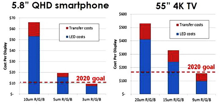 LED die and transfer cost estimates for a QHD (2560 x 1440) Smartphone and a 55” 4KTV vary strongly with die size. (Source: Yan at ADS, estimates originally from A. Paranjpe et. al. at Veeco)
Cost estimates from Professor Yan for the LED die and transfer costs are given in the figure. Note there is no time frame given to the estimates, only a 2020 goal. Clearly, to achieve this goal it is necessary to use the smallest possible microLED die in the display. Since red, green and blue LEDs are currently manufactured in large volume, the cost structure for these die is well understood.
Since assembly methods are still being developed, the cost for this transfer from the epi wafer to the backplane is poorly understood and is likely to be different for each of the many transfer methods being developed. Yield costs are not estimated in this figure and these costs are not understood at all and are not likely to be understood until the transfer processes are developed to the point where yields can be estimated or measured.
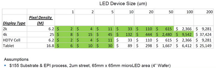 Cost of the microLED die depends strongly on size and display resolution (Source: Francois Henley at ADS)
François Henley also gave an estimate of the die cost for various die size and display resolution combinations. He has highlighted the areas he considered viable, at least in the short term. He cited Yole estimates saying the die size in the recently announced (CES 2018) Samsung 146” 4K “microLED TV” AKA “The Wall” was 125µm x 225µm, which, in fact, makes them miniLEDs, not microLEDs. With this die size, Henley estimates a total die cost for this display of about $30,000 with a die assembly cost of more than $15,000. Samsung has not announced the price of this unit yet, but it is believed it will be in the $250k – $300k range.
MicroLED manufacturing techniques
One of the defining characteristics of microLED direct view displays is the very large numbers of microLEDs involved. For example, a FHD (1920 x 1080) microLED display would involve 1920 x 1080 x 3 = 6.2M individual microLEDs that must be transferred from the epi substrate where they are made to the display backplane where they are needed. One pick-and-place mass transfer method discussed at the ADS involved transferring 60,000 die at a time every 20 seconds. For an HDTV, this would involve transferring about 104 groups of die over a time period of 35 minutes. Since no one is talking about making HDTV panels with microLEDs because it is a high-cost, premium process, a 4K UHD panel would require 25M die and 139 minutes of assembly time with this process. To make 1 million 4K panels per year it would take 395 of these machines running in parallel, each operating 16 hours a day, 365 days a year.
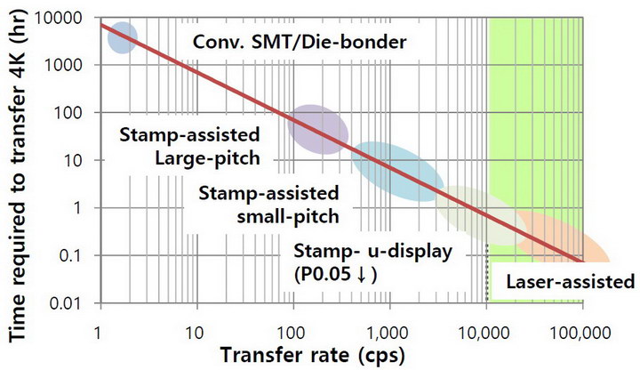 4K TV assembly time vs. transfer rate in microLEDs per second (Source: Jihoon Kang at ADS)
The figure from Jihoon Kang at Samsung shows assembly time of a 4K TV vs. transfer rate of microLEDs and includes which of several general categories of transfer methods can achieve what throughput rates. A conventional SMP/die bonder system is included on a graph, mostly to prove new methods are needed. With a system like this, making a 4K TV would take perhaps 5000 hours. This is probably not an acceptable production time, even for a one-of-a-kind prototype or demonstration unit.
This transfer must have a very high yield, both on alignment of the die to substrate and electrical connection between die and substrate, plus every epi die must also be functional. If not, epi yield must also be included in the yield equation. High yield doesn’t mean 99.9% because a yield that low would leave about 6,221 sub-pixels to be repaired in an HDTV or 24,883 to be repaired in a 4K set.
One speaker, Henley from Tesoro Scientific and QMAT, Inc, discussed a yield for good sub-pixels of seven-9’s or 99.99999%. A sub-pixel yield at this level would produce 10 FHD panels with a single sub-pixel defect per million panels and these bad panels could be discarded or recycled – no sub-pixel repair needed. For a 4K panel, there would be 42 panels per million with a sub-pixel defect. Not surprisingly, Henley did not consider a good sub-pixel yield of 99.99999% to be feasible in the foreseeable future and expected any microLED display manufacturing process to include a sub-pixel repair process.
 Sparse vs. dense arrays of microLEDs (Source: Vincent Lee at ADS)
There are two general types of microLED displays: sparse and dense, as shown in the image. In a sparse array, it is necessary to move the microLEDs to positions that are farther apart than they are on the epitaxial wafer where they are originally made. This must be done with a precision that is better than the size of the microLED. In other words, a 3µm microLED needs to be placed on the substrate with an accuracy of better than 3µm. A dense array has the same spacing as on the original epitaxial wafer.
According to Jihoon Kang at Samsung, there are three general categories of methods under development for the mass transfer of LED die to the display substrates and identified some of the companies working in each general category. These approaches for sparse arrays are:
- Stamp Systems
- Electrostatic force (Luxvue Apple)
- Elastomer (X-Celeprint, ITRI, etc.)
- Laser ablation (QMAT, Uniqarta, Sony)
- Fluidic assembly (eLux)
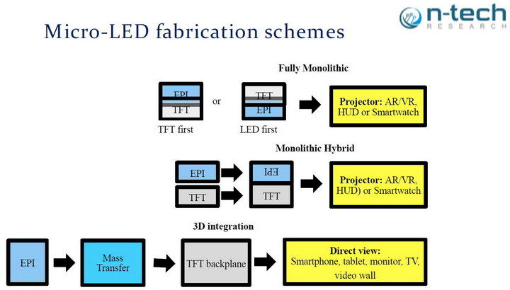 Three paths for microLED manufacturing. (Source: Boris Kobrin at ADS)
The three categories given by Kang are all in the “3D Integration” category as shown in the figure. Boris Kobrin from N-Tech Research broke this 3D integration category down further into specific, publicly known projects from companies known to be working on microLED assembly processes for sparse arrays:
- Pick-and-place transfer (Samsung, Sony)
- Electrostatic MEMS (Apple/Luxvue)
- Electrostatic stamp (Cooledge, AUO, VueReal)
- Elastomer stamp or roll (X-Celeprint, ITRI, KIMM)
- Ultrasonic/acoustic roll (Innovasonic)
- Magnetic/electromagnetic stamp (ITRI)
- Adhesive stamp (PlayNitride, Intel)
- Mechanical transfer (Rohinni)
- Thermo-mechanical laser transfer (Uniqarta)
- Laser ablation transfer (Optivate)
- Fluidic self-assembly (Nth degree, Sharp, PSI)
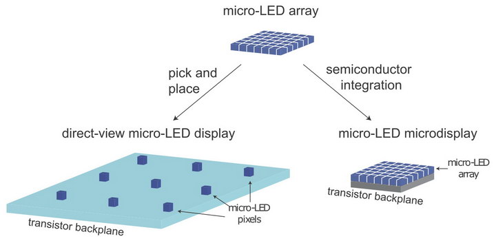
Kobrin’s list did not include the monolithic approaches that can be used for making microLED microdisplays. If you have problems bringing the microLEDs to the backplane, try bringing the backplane to the microLEDs. These methods are all based on photolithography where the creation of millions of carefully aligned devices with high yield and low cost is a day-to-day part of manufacturing life.
In general, these approaches are only suited for LED microdisplays and cannot be used to produce the sparse arrays of microLEDs needed for large displays. Smartwatches are, perhaps, the biggest displays that could be made with these methods. The methods are also only good for monochrome red, green or blue microdisplays – more on this later. These photolithographic and wafer-based methods include:
- Photolithographic formation of the TFT backplane on the LED epi wafer (Lumiode)
- Epitaxial growth of LEDs on a CMOS silicon wafer (SungkyunKwan Univ., SOLES, MIT, Allos, Plessey)
- Monolithic Hybrid Integration (JBD)
These lists of assembly projects and techniques are certainly not complete. Other companies discussed at the ADS but without enough information for me to classify them into one of the categories above include VueReal, Aledia, Glo, Quantum Photonic Imager (QPI) and Ostendo. Given the difficulty of achieving the needed chip transfer rates and the needed yields; and given the very high rewards likely for the companies that succeed; there are probably many additional microLED assembly development projects in stealth mode.
Forecasts
Boris Kobrin from n-Tech Research was the only person willing to give specific numerical forecasts for microLED displays going forward.
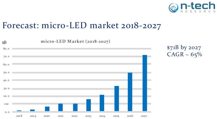 Forecast for microLEDs through 2027 from n-Tech (Source: Boris Kobrin at ADS)
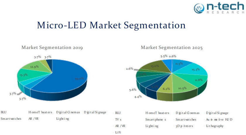 Market segmentation for microLEDs in 2019 and 2027 from n-Tech (Source: Boris Kobrin at ADS)
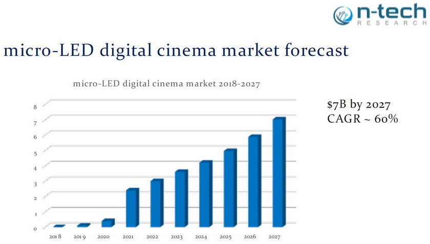 Forecast for microLEDs digital cinema through 2027 from n-Tech (Source: Boris Kobrin at ADS)
Given the uncertain state of microLED assembly technology, I don’t blame others for not giving specific forecasts for microLEDs going forward. If the technologists succeed in making microLED displays reliably and at moderate cost, whether n-Tech’s forecast is spot-on or not, the market is going to be big and will develop as soon as the manufacturing methods permit.
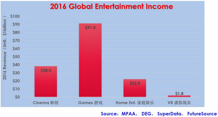 The Global Entertainment Industry in 2016 (Source: Professor Frank (Qun) Yan at ADS)
This figure on the global entertainment industry is not a forecast – it is a snapshot of the industry taken in 2016. It shows that in 2016, the entertainment industry was dominated by gaming, not the cinema or home entertainment. This trend is expected to continue and gaming is expected to be an ever-increasing force in entertainment. If someone wants to make a lot of money in microLED displays, he needs to figure out how to make a microLED display essential to gamers. Matthew Brnnesholt