It has taken me a while to appreciate that microLEDs have the potential to be much more than a brighter, less expensive, and more energy-efficient display technology. But I need to provide some background before I can justify that statement.

To start, microLEDs (or µLEDs or microILEDs) are smaller, sometimes much smaller, versions of the inorganic light-emitting diodes that appear in LCD backlights, LED signage, and other applications. The layers of the microLEDs are epitaxially grown on a base wafer. The most direct way to use microLEDs in a display is as a small microdisplay with the same, usually very fine pixel pitch they have on the epitaxial wafer. Such displays, which can have a luminance of a million (yes, a million) cd/m² or more, are being developed for projection and augmented and virtual reality applications. We’re not going to talk about these microdisplays, useful as they will be.
Things really get interesting when you remove the microLED chips and transfer them to a display substrate in a way that converts the dense matrix of the chips on the epitaxial wafers to a “sparse matrix” that provides the pixel pitch that gives us FHD, 4K, or 8K displays for smartphones, PCs, TV, or signage displays. The most popular way of doing this is with an elastomeric or MEMS-based print head that, in a process called micro transfer printing (µTP), picks up the LED chips from the wafer and deposits them on the substrate. But to create the sparse matrix on the display substrate, the print head picks up only every tenth, twentieth, or nth LED chip from the epitaxial wafer. This provides the desired pixel pitch, but since each microLED chip is so small, it might occupy only 1% of the pixel area, with the rest being empty substrate.
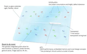
The real power of a microLED display is that the substrate can be populated with much more than microLED chips. (Graphic © X-Celeprint Ltd. 2017)
If we stopped there, we would have a display superior in a variety of ways to both LCD and OLED, but things get really interesting when we think about what can be done with all that empty space. The µTP process applies just as well to any small thing as it does to a microLED chip. One such small thing is an IC chip. A single IC chip could provided the pixel switches for multiple microLED pixels. No more TFT backplances, no more slow LTPS annealing, and now your pixel switches would have the high electron mobility of single-crystal silicon. And why stop with pixel switches? Other µTP’d ICs could provide high-level logic and information-processing functions, and a variety of sensors could also be deposited in the “dark” area. The display could evolve from a system peripheral to the system itself, and would be imbued with far more value than it is today.
My mind is blown! I need to have a glass of wine and give this a lot more thought. – Ken Werner
[Disclosure: The author is a member of the advisory committee for X-Celeprint, a microLED company. He has shown this article to X-Celeprint’s CEO to make sure it does not violate any NDA provisions. No changes were made to the article as a result of this screening.]
Ken Werner is Principal of Nutmeg Consultants, specializing in the display industry, manufacturing, technology, and applications, including mobile devices, automotive, and television. He consults for attorneys, investment analysts, and companies re-positioning themselves within the display industry or using displays in their products. He is the 2017 recipient of the Society for Information Display’s Lewis and Beatrice Winner Award. You can reach him at [email protected].