Today’s consumer electronics products rely on a wide range of technologies and engineering disciplines. However, the mechanical and materials engineering used in today’s state of the art CE products often go on unrecognized.

As a recent purchaser of a smartwatch (an Android Wear unit as I am not a member of the Apple fraternity), I was in part intrigued by the amount of OLED display, touch screen, sensors, and microelectronics packed into the device on my wrist as well as somewhat dismayed at the device’s large size. A recent teardown and analysis of the Apple Watch by our friends at Chipworks provides an excellent example of the engineering arts and sciences required to create such a wearable device.
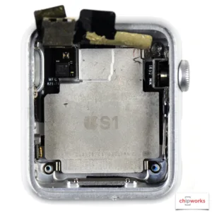
The Apple Watch contains an “S1 chip” as was described at product launch and as illustrated in the teardown photo below from Chipworks.
Source: Chipworks
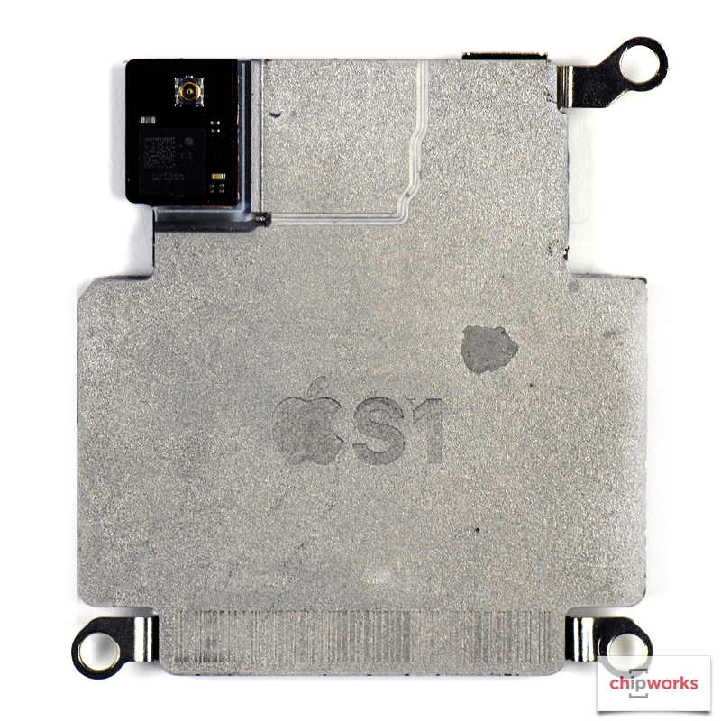
Rather than being a very large single silicon integrated circuit, the S1 is actually a system-in-package (SiP), or a complex assembly of over 30 individual chips with many additional passive components mounted on a (very dense) printed circuit board (pcb).
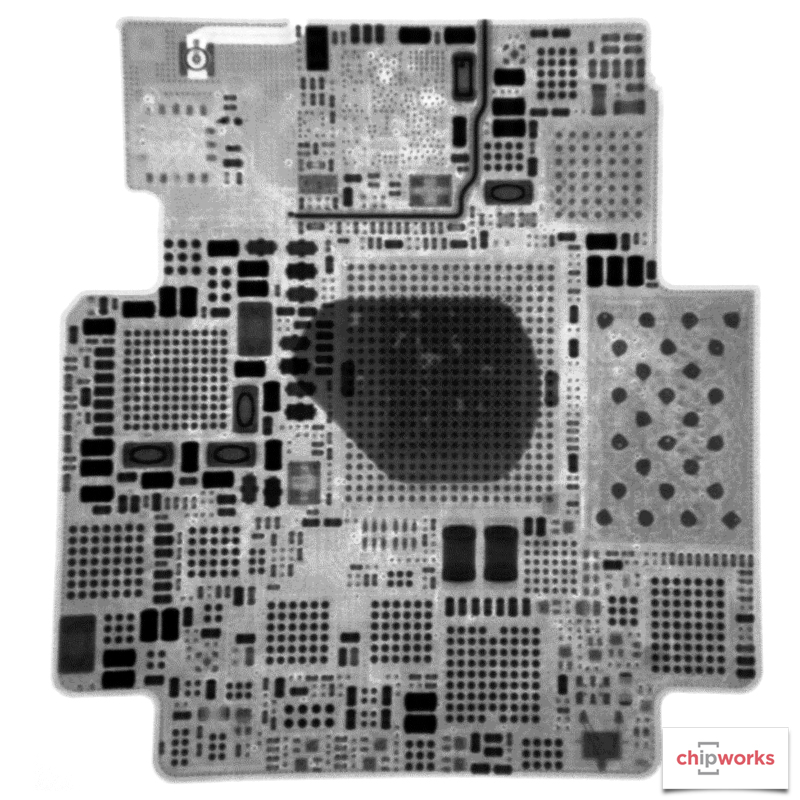
Chipworks has gone on to remove the S1 from the Apple Watch case and take an x-ray image of the SiP (images below).
 Source: Chipworks
 Source: Chipworks
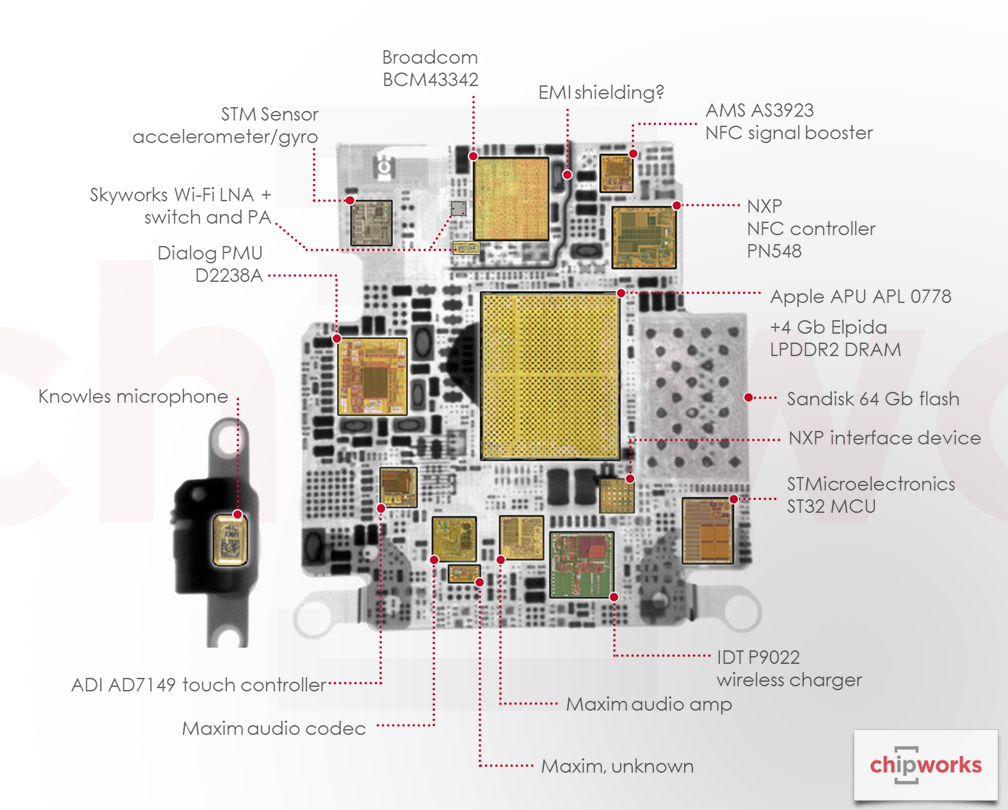
Chipworks has proceeded to identify many of the individual components as shown in the annotated macro photograph below.
 Source: Chipworks
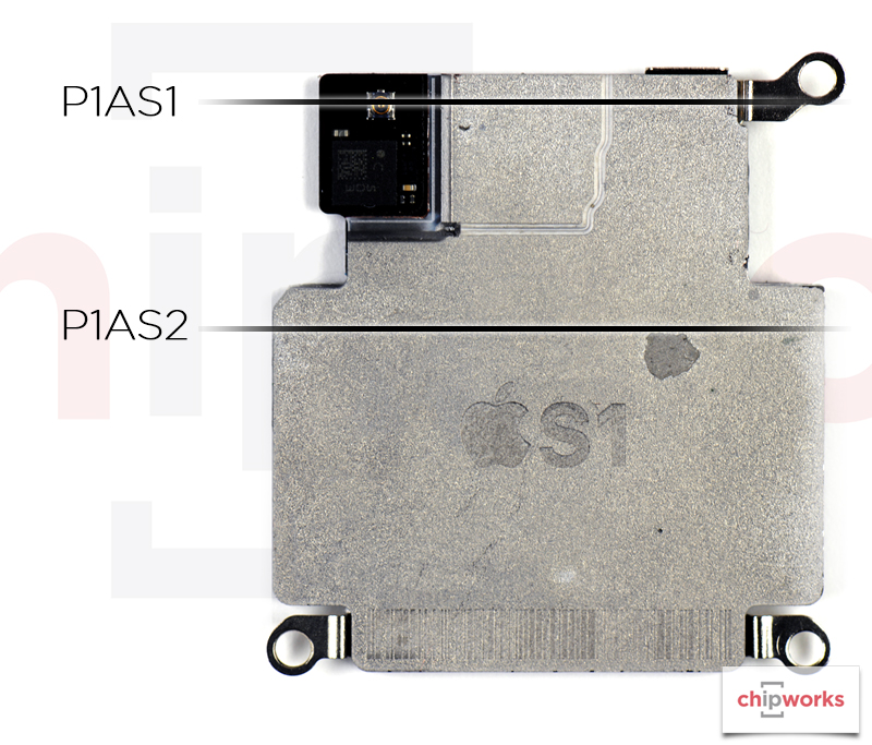
Not satisfied to halt at this level, Chipworks then prepared metallographic cross-sections at two locations of the S1 SiP (cross-sections P1AS1 and P1AS2) as shown below.
 Source: Chipworks
The cross-sections reveal in great detail the fine scale engineering of the assembled SiP. For example, the cross section below shows on the left the Dialog power management unit (PMU); in the center is the Apple application processor (APU) (APL0778), co-packaged with an Elpida DRAM; and at the right is the SanDisk 64 Gb flash, including the controller chip and a spacer die.
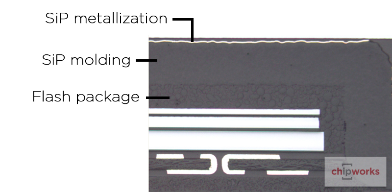
Looking closer, the micrograph below shows that while the S1 uses “conventional assembly techniques” as described by Chipworks, the components on the 4-layer pcb are then overmolded and plated with metal to give the stainless steel appearing finish evident in the photos of the S1 SiP above.
 Source: Chipworks
The micrograph above shows that there are two 32 Gb flash memory dies in a conventional package with its own substrate, which is flip-bonded onto the PCB, which is covered with the SiP over-molding. Finally, the outside of the SiP is metallized, yielding the silver appearance shown above.
The packaging and assembly engineering embodied in leading edge products like the Apple Watch exemplify many of the technological elements common to today’s consumer electronics. Based in the high level of the engineering arts and sciences applied to the Apple Watch, I am looking forward to the next generation Android Wear smartwatch which I hope will look a bit less heavy handed on my wrist. – Phil Wright