A team of researchers headed by Professor Shin Hyun-seok of the Department of Natural Science within the Department of Energy Engineering at Ulsan National Institute of Science and Technology (UNIST) (Ulsan, Republic of Korea) is developing a technology to improve the means used to fabricate graphene quantum dots.

First a few words of background information.
Graphene is a material composed of carbon atoms that are bonded in the form of a hexagon. Graphene quantum dots are semiconductor nanoparticles that have a size of several nanometers and that possess unique fluorescence emission properties. Given these emission properties, there has been considerable interest in the use of graphene quantum dots in a variety of applications that include displays.
Up to now, graphene quantum dots have typically been fabricated using a process that includes peeling thin layers of graphite from bulk material by the use of physical and chemical reactions. Unfortunately, with this method, it has not been possible to produce graphene quantum dots having a desired size. In addition, this production method results in impurities at the edges of the graphene quantum dots that impede the flow of electrons. The bottom line is that this production method prevents devices based on graphene quantum dots from using the full potential of the material’s optical and electrical capabilities.
The UNIST team has developed a novel means to address these issues. An article reporting recent results on this topic is entitled “Planar and van der Waals heterostructures for vertical tunnelling single electron transistors.” It was published in Nature Communications volume 10, Article number: 230 (2019). A copy of the article is available for download here.
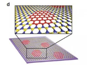
The newly developed means consist of arranging a regular array of graphene quantum dots in a single layer on a substrate containing a layer of hexagonal boron nitride. The single layer can be thought of as a two dimensional material and referred to as a heterostructure. As indicated by the name, hexagonal boron nitride is a material in which nitrogen and boron are combined in a hexagonal honeycomb shape. Since graphene and hexagonal boron nitride are similar in structure, it has proven possible to grow graphene quantum dots inside the matrix of hexagonal boron nitride.
The team’s most recent article contains detailed information on the process developed to produce the graphene quantum dots. In summary, the new means places hexagonal boron nitride on a silica substrate on which platinum nanoparticles are arrayed. The substrate is then heated in the presence of methane gas. The size of graphene quantum dots is determined by the size of the platinum particles. The synthetic process is outlined in the figure below.
The fabrication steps of graphene quantum dots – hexagonal boron nitride in-plane heterostructure based on hexagonal boron nitride to graphene conversion catalyzed by platinum nanoparticles.
Using the new method, the team reports fabricating a uniform array of graphene quantum dots. Also demonstrated was the ability to adjust the size of the graphene quantum dots from 7nm to 13nm.
In addition, it was found that impurities were minimized. The reason offered to explain this effect is that the growth of graphene quantum dots embedded in the hexagonal boron nitride sheet are chemically bonded to the boron nitride.
The team concludes their article with the statement that “We hope that our approach will pave the way for many other types of devices and physical phenomena to be studied.” –Arthur Berman
UNIST, Hyeon Suk Shin, +82-52-217-2311, [email protected]

