In my earlier article about six months ago, I summarised the six main categories of technical driver of higher performance IGZO and the rationales for higher performing (oxide) semiconductor materials in displays.

Higher performance IGZO can be attained by different levers, in general with different mechanisms: (i) process optimisation, (ii) TFT structures, (iii) crystallisation methods, (iv) changing the gates and passivation dielectrics, (v) controlling the roughness of the gate insulator and IGZO interface, and the method we are concerned with here (vi) dual or multiple layers of IGZO or constituent parts.
Recently on Atomic Layer Depostion (ALD) by the Dutch research organization TNO at Holst Centre and SALDtech, an equipment vendor in the Netherlands, has been building on research from an institute in Korea (Hanyang University in collaboration with Hosono’s group -referenced in the previous article). This work adds a new sub-bullet to this list of methods: there is an additional option to use IGZO Nanolaminates.
ALD is a method of using surface-controlled gas phase precursors to deposit thin, uniform, pin hole free and dense layers as an alternative to Plasma Enhanced Chemical Vapor Deposition (PECVD the method used to create most of the thin films in TFTs). While ALD is widely used in semiconductors, it has historically been considered to be too slow to be of any use in display making, with its targets of around a minute tact (process time) for a large substrate. This time problem has been solved with the introduction of spatial ALD.
ALD Makes a Brief Appearance
ALD made a brief appearance in interest in the display industry around 2013 with Synos’s work on the use of ALD for Thin Film Encapsulation (TFE) layers in OLED. This ultimately failed at the time, though recent work allows for Spatial ALD in the TFE (thin film encapsulation) application also.
TNO at Holst Centre in cooperation with SALDtech has shown on small samples that this approach can demonstrate mobilities of 70 cm²/Vs for transistors that have a W/L (a term related to transistor sizing) of 15 micron. (See figure 1). Their proprietary approach uses Spatial ALD which we describe below to create multiple layers of Indium oxide, gallium oxide and zinc oxide in a nanolaminate stack.
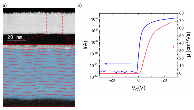 Figure 1: Recent results from TNO at Holst Centre and SALDtech for high mobility nanolaminates. A) TEM images showing the IGZO nanolaminate structure. The bottom insert illustrates the nanolaminate structure within the film. B) Transfer curve of a IGZO nanolaminate transistor (w=15 µm, l=15 µm), in blue on left axis and electron mobility in red on right axis.
With typical mass production mobility levels one fifth of this achieved level, then this is an impressive result. Higher mobility in oxide allows for potential LTPS replacement and allows for higher frame rate high density and better, narrow-bezel emissive displays.
Hanyang goes further to say that high mobility also allows for higher performance in niche display applications such as emissive microdisplays, biometrics and photosensing[1].
Nanolaminate stacks are multi-layer sandwiches of the three different oxides put down using spatial ALD in multiple very thin triads. So far TNO at Holst Centre and SALDtech have been using 15 triads of a thickness of 1-2nm each.
ALD is needed as it has much tighter thickness variation performance than PVD especially over larger areas. ALD typically has thickness uniformity of less than +/- 1%.
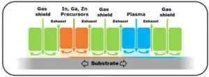
The precursors used need plasma-generated radicals to deposit a layer, hence plasma-based ALD is a requirement. In particular, SALDtech uses its spatial ALD approach using a “print head” injector which include nozzles where flows of the gaseous precursors are directed to the substrate. The substrates move under the injector and at each pass of the precursor and plasma slot one layer is formed (refer to Figure 2).
By extending the injector with more nozzles and moving the substrate back and forth the required layer thickness is achieved. With spatial ALD, deposition speeds of 1 nm/s can be achieved, limited only by the reaction speed of the precursors. Conventional or time-based ALD uses a chamber in which the gasses are let in sequentially. As the chamber needs to be purged between the gasses, the related purge time limits the deposition speed, which is in the order of one nanometer per minute for conventional ALD. As a result, spatial ALD is up to 100x faster than conventional ALD.
 Figure 2: Conceptual picture of Spatial ALD set up schematically based on narrow gas precursor supply systems
Further, by switching the precursor during the deposition process the different materials can be deposited that form the nanolaminates without exchanging the substrate. Only flushing of the precursor lines for a couple of seconds is required. The injector can also be scaled to over 2 metres in length and so it is possible to deposit Gen 8.5 or larger substrates. SALDtech has designed a cluster tool at Gen 6 which is scalable to Gen 8.5. It complies with the throughput requirements for mass production from a speed point of view.
SALDtech has two R&D tools available for companies to experiment, optimise the layers and perform process development with Spatial ALD: one for 30cm wafer-scale, as shown in Figure 3, and also standard Gen 2 (370x470mm). The process developed on these tools is one to one transferable to the production size tools.
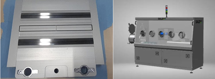 Figure 3: SALDtech’s proprietary injector on the left which is used in the 30cm wafer scale R&D tool for Spatial ALD shown on the right.
These tools allow for deposition rates of up to 0.5nm/second, thickness non-uniformity of +/- 2% with up to 3 different pre-cursor sources and deposition temperatures from 50° to 200° C.
The main growth categories in the display industry today are either high dynamic range backlighting options to support LCD or they are small and large panel emissive displays from RGB top emission small panels to WOLED+CF bottom emissive OLEDs and the soon-coming-QD OLED from Samsung.
Moreover, MicroLED is still receiving high R&D attention and could be a display technology with high visual punch, if costly. All of these markets are improved with S-ALD of high mobility oxides. The small panel options and MicroLED are applications where high performance IGZO could replace LTPS and in large panels where IGZO is already an option, then enhanced IGZO brings additional benefits. (IH)
Thanks to
Ian Hendy is a Display Strategy Consultant based in London, UK. Hendy Consulting provides growth strategy, technology strategy and deal/M&A assessments for players throughout the display value chain. SALDtech (www.saldtech.com) supplies spatial ALD tools for multiple markets and is a client of Hendy Consulting and has paid to keep this article available in front of the paywall. TNO at Holst Centre (www.holstcentre.com) is an independent research and innovation centre that develops technology addressing the global societal challenges of tomorrow and contributes to a healthier and more sustainable world
[1] Sheng et al, APS Applied Material Interfaces 2019, 11, 40300-40309