The nanoplatelets referred to in the title of this article have been described as a second generation of quantum dot material for use in applications such as LCD and LED displays.

The description was offered in a recent article published by an international team of researchers headed by Sotirios Christodoulou of the Department of Chemistry at Ghent University (Gent, Belgium). In their article, the team reports investigating the design of semiconductor nanoplatelets with the goal of developing materials that emit light with a broader range of color, provide greater luminosity and that consume less energy when compared to currently available materials.
The article is entitled “Chloride-Induced Thickness Control in CdSe Nanoplatelets.” It was published in Nano Lett., 2018, 18 (10), pp 6248-6254. A copy of the article is available for purchase here.
First, a few words of background information.
Conventional semiconductor materials typically emit light in all directions. As a result, a large portion of the emitted light can be “wasted” when such a material is used as a light source in a device. One consequence of such waste is an increase in the amount of energy consumed by the device. A common means to reduce waste is to increase the directionality of emitted light by the use of filters. This solution is, however, not ideal in that any light that does not enter the filter is still wasted.
Another means to address this issue is based on a class of semiconductor materials made with cadmium cells. Nanoplatelets composed of such materials have demonstrated the ability to absorb both ultraviolet and visible light from any direction and preferentially re-emit it perpendicular to the surface of the nanoplatelet. The directionality of the emission derives from mechanical and electrostatic phenomena that take place in the 2D geometry of these nanoscopic objects.
Since the nanoplatelets naturally emit light predominantly in the desired direction, filters are not needed and associated light and energy loss is minimized. This directionality is one of the reasons for the team’s decision to focus on nanoplatelets. A nanoplatelet and its emission pattern are illustrated in the left hand portion of the figure below.
In a related matter, as explained in the team’s article, “the semiconductor structures for optical devices heretofore offered intense and pure purple and green colors, but the output of other colors was lackluster.” More specifically, current synthesis methods typically produce nanoplatelets that emit, in discrete steps, from 460 nm to 550 nm. Clearly, additional colors are needed for device applications. The search for a solution to this issue was the subject of the team’s latest research.
In this most recent work, the researchers started with theoretical studies to model nanocrystals using so-called quantic mechanic tools. The goal was to better understand and predict the physical behavior of the nanocrystals. The team’s calculations showed that it was possible for nanoplatelets to emit light having additional colors and that this required producing thicker nanoplatelets.
Up to now, it has been found difficult to produce thicker nanoplatelets. The means currently used to do so is based on colloidal atomic layer deposition onto CdSe cores or by synthesizing nanoplatelet core/shell structures.
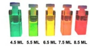
The team developed an innovative means of synthesis to produce thicker nanoplatelets. The process starts with “nanoplatelets having 4.5 monolayers and increased the thickness using a two-step reaction that switches from 2D growth to 3D growth. The key feature is the enhancement of the growth rate of basal facets by the addition of CdCl2. The process produced a series of nearly monodisperse CdSe nanoplatelets with thicknesses between 5.5 and 8.5 monolayers.”
The resulting nanoplatelet samples did indeed exhibit a broadened emission spectrum particularly in yellow, orange and red wavelengths. More specifically, the emission had peaks from 554 nm up to 625 nm and full line widths at half maximum (FWHM) of from 9 nm to 13 nm. These materials are represented as some of the narrowest colloidal nanocrystal emitters currently available in this spectral range.
The right hand portion of the figure below contains photographs of a series of nanoplatelet samples under UV illumination that have an increasing monolayer thickness.
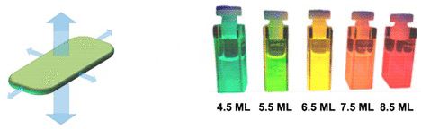 Left: a schematic representation the emission from a nanoplatelet. Right: photographs of nanoplatelet samples under UV illumination. The samples consist of a series of materials having increasing monolayer thickness.
The sample nanoplatelets exhibited a short emission lifetime of from 5 ns to 11 ns.
In their article, the researchers concluded by stating that “chloride ions can add a new degree of freedom to the growth of 2D colloidal nanocrystals, yielding new insights into both the nanoplatelet’s synthesis as well as their optoelectronic properties.” -Arthur Berman