A team of researchers from the Singapore-MIT Alliance for Research and Technology (SMART) Centre have recently published a study that showcases a groundbreaking advance in LED technology by developing the world’s smallest LED with enhanced strain sensing capabilities. The new technology has the potential to convert existing cameras in everyday devices, like smartphones, into microscopes by only modifying the silicon chip and software. This advancement has significant implications for the miniaturization of diagnostic tools in various fields, including indoor farming and sustainable agriculture.

The researchers have addressed two key technology issues with their groundbreaking LED strain sensor design: size and sensitivity. Traditionally, strain sensors are larger and may not provide accurate readings at lower strain levels. This has limited their applicability in fields such as microelectromechanical systems (MEMS), wearable technology, and biomedical devices that require precise measurements. The researchers have overcome these limitations by developing the world’s smallest LED strain sensor, which measures only 1.7 square micrometers in size, while also offering enhanced sensitivity to detect even the smallest changes in strain.
Currently, most photonic chips get light from sources outside the chip, which leads to lower energy efficiency and limits their potential. Researchers have tried various materials to create light emitters directly on the chips, but integrating these into standard chip-making processes has been challenging. Silicon, a commonly used material, has shown potential but suffers from low efficiency due to its indirect bandgap. This, along with limitations in available materials and fabrication tools, has prevented the development of a small, native silicon emitter that can be integrated into common chip-making platforms.
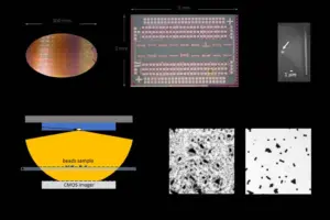
This tiny LED was used to build the world’s smallest holographic microscope. Thus, the researchers also developed a groundbreaking neural network algorithm. This algorithm can reconstruct objects that are measured by the holographic microscope, allowing for a better examination of microscopic objects like cells and bacteria without needing large, traditional microscopes or additional lenses. The research also brings us closer to a major goal in photonics: creating a powerful, ultra-small light emitter that can be integrated directly into photonic chips, which has long been a challenge in the field.
Reference
Li, Z., Xue, J., de Cea, M. et al. A sub-wavelength Si LED integrated in a CMOS platform. Nat Commun 14, 882 (2023). https://doi.org/10.1038/s41467-023-36639-1