microLED displays — displays consisting of micron-scale inorganic LED chips that are not individually packaged — have been much discussed but little seen. At Display Week, though, several microLED technology demonstrations could be seen on the show floor, at least two others were shown behind closed doors or were pulled from a briefcase, and there was extensive coverage in the technical symposium.
In his Monday seminar, “MicroLEDs: Recent Advances and Applications,” Jongseung Yoon of USC, observed that some of microLEDs’ advantages are infinite contrast ratio (like OLED), a response time in the nanoseconds (compared with microseconds for OLED and milliseconds for LCD), long lifetime, low energy consumption, high viewing angle, and extremely high pixel density.
The Canadian company VueReal, which did not appear to be represented at Display Week, reported 6000 ppi last year. That’s impressive and useful for microdisplays and projection, but for direct-view applications such as TV sets the pixel density must be much less than this. So technologies for selectively picking up microLEDs from the wafer on which they were made and depositing them on a substrate with much greater pixel spacing to make a “sparse matrix” are crucial if microLEDs are to be a major display technology for consumer electronics.
In “Status and Prospects of microLED Displays” (Paper 45.1), Eric Virey (Yole Development) and Nicolas Baron (KnowMade) said,
“Assuming traditional pick and place equipment could manipulate such small devices, those tools typically deliver processing speed of around 25,000 units per hour (UPH). At this pace, it would take more than 1 month to assemble a single display! We consider that to become cost-compatible with most consumer applications, microLED chip transfer must reach rates of about 50-100 million per hour.”
The authors mentioned X-Celeprint’s polymer stamp transfer process and Apple/Luxvue‘s electromagnetic and electrostatic MEMS approaches, and eLux’s fluidic assembly. Virey also commented that microLED chips are less efficient that LED chips of normal size, “but it just has to be better than OLED.”
In invited paper 45.2, “Micro-LED Displays: Key Manufacturing Challenges and Solutions,” Ajit Paranjpe and colleagues (Veeco) said that meeting cost targets for microLED displays will be challenging. Veeco believes:
“A two-step mass transfer approach using a dense interposer substrate or cartridge provides the benefit of maintaining low overall transfer costs while increasing epitaxy wafer usage and yield through the use of smaller transfer fields.”
In other words, instead of using micro transfer printing (µTP) to directly transfer microLED chips from the wafer to the final large display substrate, they suggest is less expensive and produces greater chip consistency if chips are extracted from a relatively small area of the wafer and deposited on a relatively small interposer substrate. Then the interposer substrates will be transferred onto the final display substrate. The paper makes a convincing argument for this approach.
Looking at Hardware
Behind closed doors, X-Celeprint showed a technology demonstration of its 5.1″ microLED Display. Until I saw the AUO display (see below), I believed this to be the largest microLED display yet constructed. The display has 70 pixels per inch, active-matrix switching using micro-ICs (not TFTs), pixel-level compensation, subjectively very high contrast, and highly saturated colors including a very red red.
X-Celelprint has accumulated an extensive IP portfolio on µTP, including the transfer of microLED chips and the transfer of microcircuits and other small objects. The company intends to spin off a new company devoted exclusively to displays within the next 12 months. (Disclosure: The author is a member of an X-Celeprint advisory committee, for which he is paid modestly — very modestly.)
In a private conversation, Graham Woodgate and Paul May updated me on Optovate. (Optovate Comes out of Stealth Mode). Founded by former Sharp and CDT people some years ago, the company acquired significant IP only to find that nobody was interested in microLED displays at the time. Now, interest is high, and the company is being re-energized. Optovate’s IP focuses on two areas. The first is removing the LED chips from their wafer via patterned laser lift-off (p-LLO) rather than using a sacrificial layer process that removes all off the LEDs from the wafer at once, with chip selection relegated to a separate step. (Be warned: There is a lot of technology hiding under that sentence.) The second major focus is sheets of catadioptric optics for controlling the angular emission of the LEDs. One application is thin miniLED backlights for LCDs that rival OLEDs in thickness and function. MiniLED backlit displays appeared in several booths on the show floor, and Paul May said Optovate was receiving “lots of interest on optics part now.”
AUO won the Best in Show Award in the medium exhibit category, in part for its 8″, full-color microLED with 1280 x 480 pixels (Fig. 1). AUO’s Norio Sugiura said each LED measured less than 30µ, and that the display was driven with an LTPS backplane. The display uses color conversion technology, which means it uses only blue microLEDs and presumably obtains red and green with phosphors or quantum dots. I asked if the display uses a mass transfer technique (such as µTP) or whether it was assembled from relatively large sections of two or more LED wafers. (The latter approach would be expensive and totally impractical for volume production, but it could be a way of getting a demo to the show floor if you had not yet mastered an appropriate mass-transfer technology.) Sugiura would only say, “That is a very good question.”
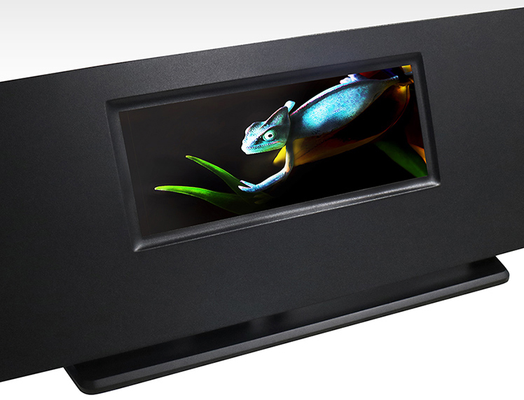 1. AUO’s 8-inch µLED display is the largest shown to date. (Photo: AUO)
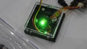
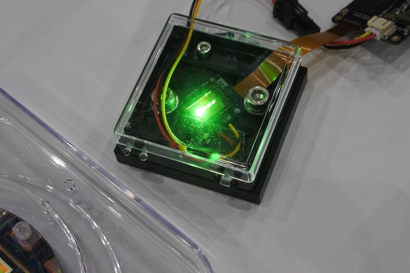
Hong Kong Beida Jade Bird Display, an I-Zone honoree, showed a green microLED display with 3 million — yes, million — cd/m² (Fig. 2). This first-generation, proof-of-concept display measured 0.65″ on the diagonal, had a pixel pitch of 20 µm, and pixel dimensions of 640 x 480. A different chip had had 2560 x 1920 pixels. The company started in 2015 and Jade Bird is targeting its displays for projection.
Taiwanese company PlayNitride was also an I-Zone honoree or “utilizing its PixeLED display technology to build a transparent display with an innovative and unique process to transfer RGB microLEDs onto a pixel.” The company, established in 2014, is a fabless company focusing on galium nitride microLEDs, which the company says it can make at pixel densities up 1500 ppi. In April 2017, there were rumors that Samsung Display was interested in acquiring PlayNitride (Samsung and PlayNitride Acquisition Talks in Final Stages?). In April 2018, the rumor was that PlayNitride was discussing a cooperative arrangement with Apple. Well, an Apple rumor is always a good way of making your investors more patient.
There was lots of microLED activity at Display Week, and lots of work remains to be done. Companies such as Jade Bird and New York start-up Lumiode (www.lumiode.com), which are focusing on µdisplays and don’t have to tackle micro-transfer issues, have a shorter path to commercialization. But they are also leaving the largest markets on the table. — Ken Werner