In the mid-2010s, at a Department of Energy workshop on solid-state lighting, a young MicroLED entrepreneur told the OLED gathering in a Khrushchev-like statement that his company would bury OLEDs by producing a commercial, cost-competitive 65-inch TV by 2020. Ten years later, the only commercial MicroLED TV costs a whopping $100,000 and is the only volume product on the market using the technology. That entrepreneur, Charles Li, CEO of PlayNitride, has taken his company public and for the first time reported an annual profit. PlayNitride supplies MicroLEDs for Samsung’s Wall TVs, where the size and cost of the devices are not critical. He came to Display Week 2025, sans TV, to participate in a panel discussion on the status of the Micro LED industry.
The leaders of the MicroLED industry took center stage at the conference with a panel consisting of:
- Eric Virey, Principal Display Market and Technologies Analyst and Consultant, Yole Group, moderator
- Wei-Lung Liau, CTO, AUO
- Alex Chen, CTO, BOE
- Charles Li, CEO, PlayNitride
Shockingly, the takeaway from the panel discussion was that very little had changed over the past 10 years. MicroLEDs were still too large and too expensive. Mass transfer still lacked a viable solution that could balance the offsetting requirements for small devices, accurate placement, high yields and high throughput. The industry still needed a viable approach to binning and error correction, as well as competitive external quantum efficiency as die sizes are reduced.
Compounding the challenge is that LCDs and OLEDs have made major improvements to reduce or eliminate differences in performance and exaggerate cost differences:
LCD TVs with MiniLED backlights broke the 10,000-nit luminance goal and reduced costs by more than half. There is excess capacity, and a 32-inch 4K TV open-cell panel is priced at $37 while a 14-inch 2K IPS module is priced at $46.
OLEDs have doubled their efficiency over the last five years to more than 25% EQE without phosphorescent blue and promise another doubling in the next five years. Panels are built on fully depreciated fabs, and luminance for TVs is more than 4,000 nits.
Although the panelists pointed to markets for TVs, watches, automotive and other displays, there is only a small available niche market left as LCD costs are unmatchable and OLED panel performance and costs tend to block new competitors at the high end.
A second approach, not covered by the panel but espoused by Jade Display, Aledia and others, is to wait for AR to mature, hoping that Laser Beam Scanning, being developed by Microsoft and Meta, will not outperform LEDoS.
A third approach is to look for opportunities where MicroLEDs are unique, such as in delivering light with very small devices that leave room for added functionality and do not require multibillion-dollar fabs, where micro devices can be deposited on low-cost substrates such as glass with built-in passive electrodes currently used in vehicles. This approach is being pursued by VueReal using their low-cost cartridge printer, with initial products being a variety of automotive lighting by 2027.
Chris Chinnock reported on the panel discussion: Both BOE and PlayNitride are fabricating blue and green MicroLEDs on 4-inch or 6-inch sapphire substrates. Chen said the quality of the 6-inch is better than the 4-inch, but it will take more time to reduce costs. They claimed that the cost of MiroLEDs is still over 50% of the display. A recent survey put the current cost of 1 million 20-micron LEDs at approximately $150. The participants claimed that the task is a mixture of reducing device size, improving yield and reaching scale.
- AUO’s Liau sees chip costs (PlayNitride is their major supplier) as the No. 1 driver, with mass transfer as No. 2.
- BOE’s Chen agrees on chip cost as the most important cost driver, with the second being defective detection and repair.
- PlayNitride’s Li believes capacity and a reasonable cost structure are needed to move forward.
- Yole’s Virey sees the size plateauing at 15×30 or 20×40 micron device sizes. Liau noted that as devices get smaller, in addition to the yield loss, there can be losses in efficiency, which means power consumption would go up to maintain the same luminance levels.
Chen thinks that the 15×30 micron size is best for mass transfer now, but they would consider moving to 10×20 micron flip chip. Longer term, a vertical MicroLED (stacked MicroLED) is a good direction, but it needs more research, especially regarding mass transfer and repair concerns. Li expressed a bit of frustration with the industry as customers tend to discuss options too long and not lock down specifications in terms of the MicroLED specs, TFT technology, optics, transfer equipment, etc. “Potentially, there is no limit for device size reduction—we just need to lock down a size to focus on the qualification of devices to move projects forward,” Li said. It is not urgent to reduce device size right now, he thinks; all aspects of manufacturing need to be reduced simultaneously.
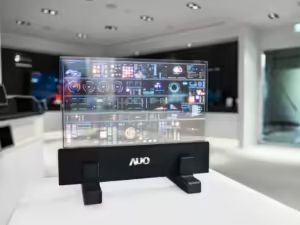
The conversation then turned to substrate size for mass transfer, where developers have been using Gen 2.5 fabs, although AUO is converting a Gen 4.5 line, which enables the production of 42-inch MicroLED modules, the biggest in the industry. To create a 127-inch home cinema screen requires eight panels in this case. The speakers acknowledged that larger-sized substrates will help reduce costs, but the industry is not ready to move to Gen 6 or Gen 8.5 yet as mass transfer is not mature.
BOE’s Chen believes Gen 6 may be a good sweet spot as LTPS offers the best driving circuit technology but agrees that mass transfer at this size is not available. For Gen 8.5, both AUO and BOE believe oxide backplanes are needed, but the mobility would need to improve from 20-30 cm²/V·sec to greater than 50 cm²/V·sec, a goal of the OLED industry as well. Oxide devices fit mid-tier MicroLED applications, which have lower resolution and brightness than LTPS-based devices. LTPS is still the best today for higher-end applications like higher brightness, resolution, transparency or frame rate. MicroIC solutions would be even more expensive, Liau thinks.
Li suggested using Gen 6 backplanes that are cut to Gen 4.5 sizes for mass transfer. He also thinks there is potential to make transistors using gallium nitride. They would like to see equipment makers increase development in mass transfer, but current volumes and market penetration won’t justify the investment. “We need customers and equipment makers to buy into this market and invest to move it forward,” Li said.
Barry Young has been a notable presence in the display world since 1997, when he helped grow DisplaySearch, a research firm that quickly became the go-to source for display market information. As one of the most influential analysts in the flat-panel display industry, Barry continued his impact after the NPD Group acquired DisplaySearch in 2005. He is the managing director of the OLED Association (OLED-A), an industry organization that aims to promote, market, and accelerate the development of OLED technology and products.