Several micro LED companies received funding recently, an encouraging sign of the continuing interest in this segment. But in a new report from Yole looking at the patent situation, the authors warn that things will be messy – especially for displays that require a mass transfer approach.

Let’s start with the funding news. Samsung has announced a long-term agreement with San’an Optoelectronics, who is apparently one of China’s largest LED suppliers. Samsung has now agreed to pay the company $16.83M to secure “micro LED chips.” The agreement spans three years and it will take some time to scale to mass production, but this is a decent commitment to the technology.
Exactly what the companies mean by micro LED is debatable, however. Samsung seems to define micro LEDs as devices and/or pixel pitch of under 1mm. This is consistent with the demonstration of the 146” Wall display at CES which was labelled a micro LED platform. Samsung has also been rumored to be tied up with Taiwan-based PlayNitride, another micro LED developer.
LETI spinoff Aledia has also received new funding to the tune of $36M in a C round with Intel Capital joining in. A and B rounds in 2013 and 2015 raised an additional $40M. The new round will help speed development including the purchase of new equipment.
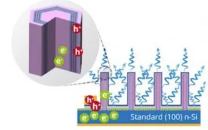
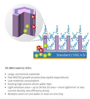
Aledia is developing a rather novel emissive approach where GaN nanowires are grown vertically on a silicon substrate. This is a monolithic approach allowing the entire backplane to be fabricated in silicon with dozens or hundreds of GaN nanowires fabricated next for each pixel in the display. Each nanowire has a quantum well structure which controls the emission wavelength. Aledia is focused on blue emission for now relying on other technologies like phosphors or quantum dots to create the red and green light needed to make a display. But just controlling the growth of the nanowire emitters in large quantities with a high degree of precision and control does not sound that easy to me – let alone solving the color conversion problem (also see Aledia Uses Nanowires for MicroLEDs).
UK-based Seren Photonics successfully completed the first tranche of a £1 million investment round with funding from existing and new investors. This company is developing a process that grows epitaxial layers of semi-polar GaN (11-22) on m-plane sapphire and non-polar GaN (11-20) on r-plane sapphire. The main target is for green LEDs and micro LEDs, but yellow and amber LEDs are possible too.
This approach is said to overcomes two big problems typical of GaN LEDs fabricated using a polar (c-plane) orientation on sapphire substrates. One is the efficiency droop in blue LEDs which means the harder you drive the LED the less efficient it becomes after a certain level. The second is the low efficiency of existing green LEDs, mainly the result of defects, which are much lower in the semi-polar approach. The funding will be used to help continue commercialization of this technology on standard 2”, 4” and 6” sapphire substrates.
Turning to the patent situation, Bob summarized the report nicely in a recent Display Daily (Yole Looks at MicroLED Patent Developments). In terms of number of patents (not clear if issued or issued plus applications), Apple subsidiary Luxvue leads with 62, but number 3 is Facebook, interestingly.
They also found that the supply chain is very complicated and long, especially for the mass transfer category, but may be more controllable for the monolithic approach. The bottom line: it may be very difficult for companies to have full control of the supply chain and IP in the near term. On the other hand, there are so many different approaches under development right now that it is unclear which approaches will gain traction. This will be fun to watch.