Kubos Semiconductors, a UK-based developer of MicroLED material technology, has recently been selected as a recipient of a £700,000 ($892,000) Future Economy Investor Partnerships (FEIP) grant. This award has been given to the firm by Innovate UK, the British government’s agency focused on fostering innovation. The grant’s issuance hinges upon the finalization of a complementary investment spearheaded by the Development Bank of Wales.
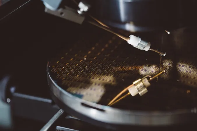
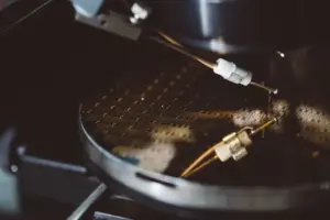
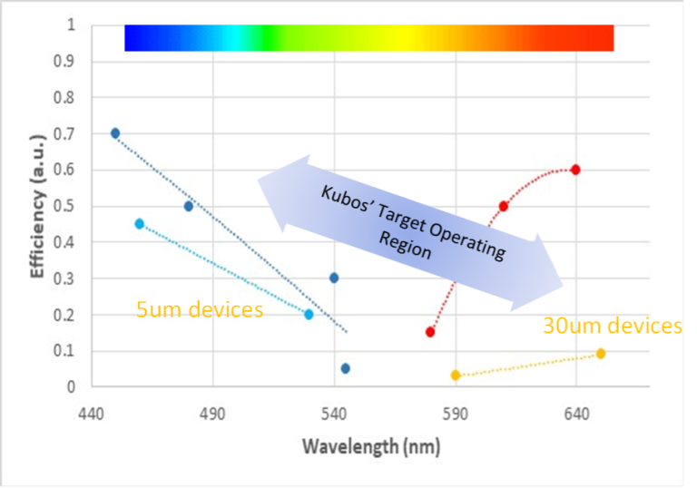
Kubos will use the funding in a two-year venture aimed at obtaining a 5% efficiency rate for their red MicroLEDs. This goal is intended to be realized through the application of their own novel cubic Gallium Nitride (GaN) process, named KubosLED.
| Feature | Cubic GaN | Standard Hex-GaN |
|---|---|---|
| High efficiency achievable (>550nm) | Yes | No |
| QCSE eliminated | Yes | No |
| Indium content (as a function of wavelength) | Low | High |
| Carrier Lifetime | Short | long |
| Colour conversion (QDs) required for Red/Green | No | Yes |
| Droop effect | Low | High |
| Blue shift effect at longer wavelengths | Low | High |
Carl Griffiths, Technology Seed Fund Manager for DBW, expressed his excitement at Kubos’ potential, noting that the company demonstrated a strong focus on deep tech, the right momentum, and a promising profile to secure the funding. He added that the burgeoning new technology possessed a defined objective and a vast market opportunity.
Upon the successful closing of the funding round in the coming fall, Kubos, as a fabless semiconductor company, is slated to inaugurate a development branch in Wales. This strategic move is projected to enable Kubos to build upon its long-standing collaboration with the South Wales Compound Semiconductor cluster, specifically the Compound Semiconductor Centre (CSC) and the Institute of Compound Semiconductors at Cardiff University, where the firm’s LEDs undergo processing and testing.
In a landmark development, the company’s foundational cubic GaN process and product technology patent has been granted in prominent markets including China, Japan, Singapore, and the US. Kubos has also broadened its patent portfolio to encompass silicon carbide epitaxy, which it employs as a growth substrate. To round off these remarkable achievements, the company has secured its first major client for its KubosLED material for use in red MicroLEDs.