Jade Bird Display Limited (Shanghai, China) or JBD has announced that the company is developing a single chip, native full color microLED display. The new microdisplay is targeted for applications that include augmented reality glasses.

Most available information on the new microLED was found in a recent company press release. Drawing upon this press release and also the company website, here is some background information related to the new microdisplay and on related light engine technology.
Several approaches are under development or are in use as the basis of state of the art, high resolution, full color microLED displays. The first approach uses three monochrome microLEDs. One microLED is located in each of separate red, green and blue color channels. The channels are combined into a full color image by the use of an X-cube.
A second approach uses a single microLED display that contains red, green and blue sub-pixels. An important advantage of the second approach is that it offers the potential to reduce the physical size of the light engine. One of the reasons that this second approach has not been commercialized is due to the fact that pick and place technology, such as that used to fabricate large sized displays, is not suited for the fabrication of high resolution microdisplays.
A third approach is based on color conversion using quantum dots. One problem with the third approach is that it typically results in a device having low power efficiency due to losses associated with light absorption. In addition, the device lifetime may be insufficient due to the high light flux typical of augmented reality applications.
A fourth approach is based on native color RGB microLEDs grown by selective area epitaxy. (Native color means no color conversion.) At this time, however, microLEDs utilizing this technology have yet been able to meet all the image quality requirements needed for commercialization.
JBD’s Approach
The approach used by JBD to address these technical issues and produce a high resolution, full color microLED display utilizes proprietary epitaxy and chip integration technologies. In this process, ultra-thin InGaN and AlInGaP epitaxy are integrated together and fabricated using conventional III-V thin-film processes.
The company explains that sub-pixels that have high energy efficiency were achieved using a patented technology in which the epitaxy layers were designed to be less susceptibility to edge effects, a problem that increases as pixel size decreases. A second success of the JBD approach was effective mesa sidewall passivation.
JBD’s new microLED display is projected to have the following specifications:
- 0.22 inch diagonal
- Native RGB colors
- qHD resolution (960 x 540 pixels)
- 5 ?m color pixel pitch (corresponding to a 2.5 ?m monochrome R, G and B sub-pixel pitch or approximately 5,000 PPI)
- Single chip (monolithic) display
It might be mentioned that a monolithic LED array can be defined as
“a single LED chip comprising multiple emitters. Each emitter has a separately addressable connection or is arranged in an X, Y addressable matrix. The emitting area can vary in width, while the formats, shapes and spacing can be designed and produced to meet specific requirements. Monolithic LED arrays are produced in a similar manner to ICs on a complete epitaxial wafer.”
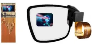
The figure below illustrates the company’s new 0.22 inch monolithic full color microLED display and a conceptual waveguide based projector incorporating the new microLED.
A 0.22 inch monolithic full color microLED display (left) and a waveguide based projector utilizing the new microLED display (right).
Other aspects of the technologies utilized by JBD in the company’s microLED and light engine products include the following.
JBD microLED displays are “manufactured in a wafer level process using standard semiconductor lithography process.? The III-V semiconductor wafer after epitaxial growth is bonded to the Intelligent Silicon-IC backplane to create microLED dice on a wafer level which are singulated and packaged as a microdisplay.? This process is called monolithic hybrid integration and enables the mass production of high pixel density displays (claimed to be up to 10,000 PPI) with pixel pitch as small as 2.5 µm.” In fact, next on the company’s development schedule is a microLED display with 3 ?m color pixel pitch (about 8,500 PPI).
High PPI microdisplays are almost always used in conjunction with collimating, projection or magnifying optics. Part of the reason that this is needed is that “the inherent light distribution of microLED displays is near Lambertian. To ensure optimum coupling efficiency with optics, JBD uses an array of micro lens. The lenses are created using standard lithography processes and serve to collimate the distribution of the light produced by the display. JBD micro lens technology is called Pixel Optics and results in the capture of almost three times the amount of light within a solid angle of 20 degrees as compared to a near Lambertian emission.”
JBD microLED products are manufactured in the company’s Hefei (China) fab as will the new, native full color microLEDs. The Hefei plant is planned to have an annual production capacity of 120 million microLED displays.
Prototypes of the new microdisplay are not expected to be available until 2023. – Arthur Berman
Jade Bird Display, Leon Baruah, +441752221827, [email protected]