A few months ago I wrote a Display Daily article about the challenges in driving microLEDs. It’s only one of a number of challenges, but in the last three months, I have had a lot of feedback on significant challenges being overcome.

Going back a year or two, there were a number of significant challenges to the development of microLED technology, each of which was a potential show stopper. The main ones were:
- LEDs are of variable quality in terms of brightness and colour. That makes it much harder to make displays as even and homogenous as viewers want and is the reason for the whole ‘binning’ process in large LED display manufacturing
- You need a lot of LEDs to make a 4K or, even worse, an 8K TV. To get the cost down, the LEDs have to be really, really small. However, as the microLEDs get smaller, they have typically got radically less efficient
- You need to transfer those tiny LEDs to a substrate
- Driving LEDs is much trickier than driving OLEDs or LCDs, so that is a challenge
 In recent weeks, I have heard that there has been progress in several of these areas and I managed to catch up with Eric Virey, an analyst from Yole Développement which has established itself as a very credible source of analysis and research on microLED and recently he gave a talk at the IMID event in Korea.
So let’s look at these issues.
Variable Quality
I heard from Virey and also from Dr Boris Kobrin of N-Tech Research (n-tech Research Issues New Report on Global Micro-LED Market – subscription required) a few weeks ago that the variability issue is not solved, yet, but is said to be close. The key is improving the homogeneity of the vapour deposition process used to make the LED wafers. Both analysts are confident that the makers of the MOCVD equipment (I believe that Veeco and Aixtron are be the strongest historic suppliers although Chinese companies are growing) are confident that the next generation of machines will be able to make LEDs that are much more consistent based on process improvements. That might solve some of the potential quality issues of microLED.
A number of companies are working on ways to analyse quality on the LED wafer and that could helpful in getting to production yields. Virey told us that one approach being considered is to use a two stage process for distribution of the LEDs that takes small areas of the wafer and scales up the area (more later in this post). If you know that whole areas of the wafer are below the required quality or performance, you can simply miss out those areas when you do the first transfer, rather than trying to work at the individual LED level. Some vendors are still confident that a method of transferring all LEDs, then repairing, is the most effective, but Virey is not currently convinced (and nor am I!).
Efficiency Reduces with Size
One of the great attractions of microLED is that the devices are very efficient in converting electricity into light – hence their use in lighting. However, in the past, once you got down to very small sizes (for example, below 10 microns per side), the efficiency drops rapidly. Part of the reason for that is that there are edge issues that had simply not been addressed in the past, as LEDs weren’t being made that small. Recently, improved designs and technology have been brought in to the field and this problem seems to have been solved, at least by some, Virey told us. PlayNitride (widely rumoured to be working with Samsung), Gl? and X-Celeprint have all reported external quantum efficiency (the number of photons given the number of electrons injected – EQE) of 35% or more – plenty good enough to make microLED the most efficient high resolution display.
Transfer
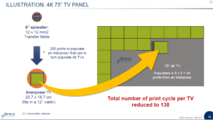
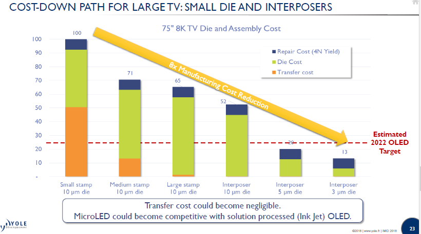
Transfer at low cost and high speed remains a challenge, Virey told us, but one approach is to use a two stage process, where the first process takes the LEDs from a small area to an ‘interposer’ that is then used to feed the final distribution process (the intermediate stage could also be used for quality control). For example, you could take 12mm square area of LEDs that would be moved to a 20 cm square interposer that is then used to populate a TV. There would be up to 255 small areas from a 6″ wafer and then the LEDs could be used to populate 46 4K TVs. Each TV would take 138 print steps in total.
If you could use this kind of process and get chip size down to below 10 microns, and perhaps down to 3 microns, Virey believes that you might be able to compete with the cost levels of OLEDs by around 2022. Competing with OLED might enable microLED to enter the smartphone display market as LED should offer higher levels of efficiency, so longer battery life.
 This is one scenario that Virey can foresee.
Driving
Since my article about driving LEDs, I have had discussions with a number of companies that are confident that the driving issues are solvable and one of those is Macroblock, which supplies a lot of the drivers used in big LED walls – and they should know! I have also heard rumours (that Virey has heard as well) that the Samsung ‘Wall’ LED is using LTPS substrates as the driving technology. If that is possible, then things look very positive for smaller display applications. However, it is always very difficult to tile displays completely seamlessly (the Samsung Wall at IFA had visible bright and dark lines between some of the panels – a bit of an issue for a €300,000 or €400,000 display, in my opinion!)
We’re Nearly There!
Finally, Virey said that the industry is now at the point where demonstrations can and have been made, and we’re started on the process of getting costs and scale right – the last 20% of the problem.
Early applications are likely to be in very large TVs, where both OLED and LCD are challenged. LED display costs scale with resolution, not area, so a 140″ UltraHD microLED TV should cost not much more than a 75″ – hence the Samsung ‘Wall’.
However, I was reminded that we first reported that inkjet OLED had reached the point of having demoes and being ‘close to a breakthrough’ when David Fyfe, then of CDT, said at a conference we ran in 2003 that, along with Epson and then Litrex, CDT was ‘close to a breakthrough’ on inkjet OLED and in 2001 it had shown ink-jet printed OLEDs. However, there are still no high volume commercial inkjet OLEDs (although Joled is ‘Nearly there’).
That last 20% can be very difficult in the display business! – Bob Raikes