I recently had a chance to speak with executives from a new company, Taiwan-based INT Tech, which is short for Innovation and Transformation. They are a technology development house that has created AMOLED displays on glass with an industry-leading 2228 pixels per inch (ppi).

That’s in the range of AMOLED on silicon substrates and 4-5X higher density than conventional AMOLED displays for smartphones fabricated on glass substrates (Samsung S8 display is around 572 ppi).
Called Ultra-High Pixel Density (UHPD) technology by the company, founder and Chairman David Chu explained that they use a low temperature poly-silicon backplane technology with an RGB (not white OLED and color filter) technology for the frontplane. But Chu would not say exactly how they are able to fabricate transistors in LTPS with such high density. Nor would he divulge the fabrication process for the RGB OLED layers, although an inkjet process seems highly likely as I don’t think a fine-metal-mask process can be used at that density. Such details are reserved for potential partners and licensees, Chu explained. But the technology is real, he confirmed, as they plan to show a 2,228ppi glass-based AMOLED at CES 2019.
INT published a poster paper at the 2018 DisplayWeek symposium which provides a few more details on their technology. Apparently, the backplane includes the gate driving circuits for the pixel array and adds a compensation circuit to account for variances in threshold voltage and allows a uniform luminance level over the entire array. It seems that the company is using a much smaller design rule to shrink the size of the pixel transistors than with conventional smartphone displays, that use a design rule in the 3-micron range. This can compromise performance, but the team claims to have achieved 33 cm²/Vs in devices with 1.5 microsecond rise times and 2 microsecond fall times, which should be quite adequate.
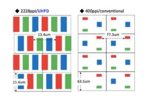
For the frontplane, INT has done a great job in increasing the aperture ratio or emitting area of their displays. The pixel layout compared to a more conventional smartphone display is shown in the graphic below. Their vertical pixel pitch calculation seems fine, but the horizontal pitch graphic seems wrong as one side should cover the width of the red pixel. Note that this is also a triad configuration and INT appears to be using sub-pixel rendering techniques to achieve the stated resolution. While ICDM has procedures to measure resolution when sub-pixel rendering is used, there can also be some room for interpretation.
In addition, Chu says they have developed what they call Smart Pixel IC (SPIC) technology. Here, the idea is to use the high-density backplane technology, but not fill it so densely with OLED pixels. Instead, the device could feature a less-dense OLED display, allowing for other elements to be placed between the OLED pixels. Chu says they are looking at adding multiple sensors including fingerprint, eye tracking, ambient light, proximity and other sensors, on the same backplane as the display. This could be very useful for Internet of Things (IoT) and biosensor applications. While this sounds wonderful, these sensors require different materials to be integrated with the LPTS backplane, which will be non-trivial to accomplish.
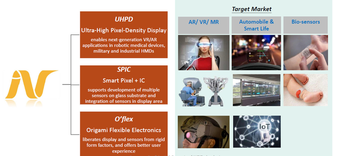
Finally, Chu explained that both the UHPD and SPIC technologies are now working on glass substrates, but they are also working to develop them to work on flexible polyimide substrates as well. The graphic below summarizes these three areas of development along with benefits and target applications.

INT’s business model is one we more often see in US or European-based companies – i.e. develop core technology but don’t plan to do the commercialization and mass production in-house. Instead, the idea is to form any number of business relationships including partnerships, joint ventures or licensing deals.
As an example of how such deals might work, Chu pointed to their first joint venture in 2017. In this case, fabless IC design company UltraChip formed a JV with INT to develop driver ICs for AMOLED displays. The JV company, called UltraDisplay, is now offering such driver chips to industry players.
Chu has a lot of experience with OLEDs, too. Until he formed INT in 2016, he was the CEO of OLED panel maker Everdisplay. They also have a strong design and intellectual property team. As of November 2018, INT has applied for 162 patents worldwide and 52 of them have already been granted, ranking them in the top 100 for patent application in Taiwan in 2017.
Before INT, there used to be a big gap in pixel density between OLED-on-silicon and OLED-on-glass displays. Not anymore. – CC

