 Giorgio Anania is from Aledia, a company that makes nanowire LEDs which can offer higher brightness, resolution and efficiency than current displays. 2D microLEDs could be very disruptive, he believes, but there are a number of barriers to overcome to bring the technology to market.
Aledia is based in Grenoble, France and is a spin-out from LETI. It has been financed to a level of $40 million and has been running for nearly six years.
To be three times cheaper than traditional LEDs is the plan for the firm. It has 95 patent families, filed or licensed. GaN LEDs have to be made hot and its difficult to do, so the company is working on a nanowire system. You can grow wires on a range of substrates, but silicon is OK, which means you can exploit the existing silicon wafer supply chain. The firm is the only one that can make GaN nanowires on 8″ silicon wafers. The nanowires are GaN but you only use a small amount compared to GaN LEDs.
Anania showed a 1″ LED – probably the biggest in the world, he said. You can make wires from GaN on sapphire, but this has the same costs as regular LEDs. If you try to make them on silicon, usually the wires are very varied in length, but Aledia has worked out how to make them very consistent. In a 2 x 2 cm, it can make 400K pixels. As Glo had said in a previous talk, there is a lot of inherent redundancy and that makes it reliable. The base cost for Aledia is around $1.50 per sq cm and Anania said that a display module would cost around $3.00 – $3.50 per sq cm, although you would have to add driver cost.
Tests so far are very good with uniformity and colour also showing very good results. The company can go up to 300mm substrates and Aledia believes that they are the only ones that can make on 300mm silicon. That’s significant because it is the size of wafer being used by the latest generations of semiconductor fabs and lots of the semiconductor tools are only available for 300mm. Aleida grows the wires, but the manufacture of the LEDs themselves is by regular chip makers so Aledia’s business model is close to a fabless model.
LED has very high brightness with up to 70% ‘wall-plug’ efficiency in lighting applications – and that compares to 5%-6% for LCDs and OLEDs and is a fundamental strength.
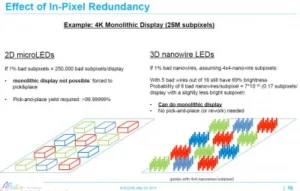
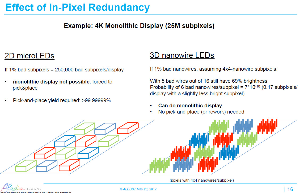 Nanowire LEDs have ‘in pixel redundancy’ to improve yields.
LEDs always have dead pixels, so building monolithic displays based on LED is ‘impossible’, Anania said. High resolution is difficult because 2D (traditional) LEDs get less efficient. Anania said that 2D LEDs need ‘7 nines’ of yield to be efficient in yield. However, for nanowires, you can have multiple nanowires fail and still have very consistent brightness.in the display.
You can go to big chips if you have big wafers – 2″ wafers can’t make big chips, he said. Aledia also believes that nanowires can be pumped much harder than 2D LEDs as there is more surface area. That means that you can go up to 107 cd/m², the firm believes. That means that the LEDs can be used for projection devices as well as direct view in very high ambient, or with lossy optics.
If you make devices with 30 micron size, you can make 400ppi. Today, the technology can make 30 micron devices and so applications such as smartwatches etc are possible. In one year, the compnay plans to be at 5 microns, which would be 2400ppi, but the company believes that more than 5,000ppi is possible with its process, eventually.
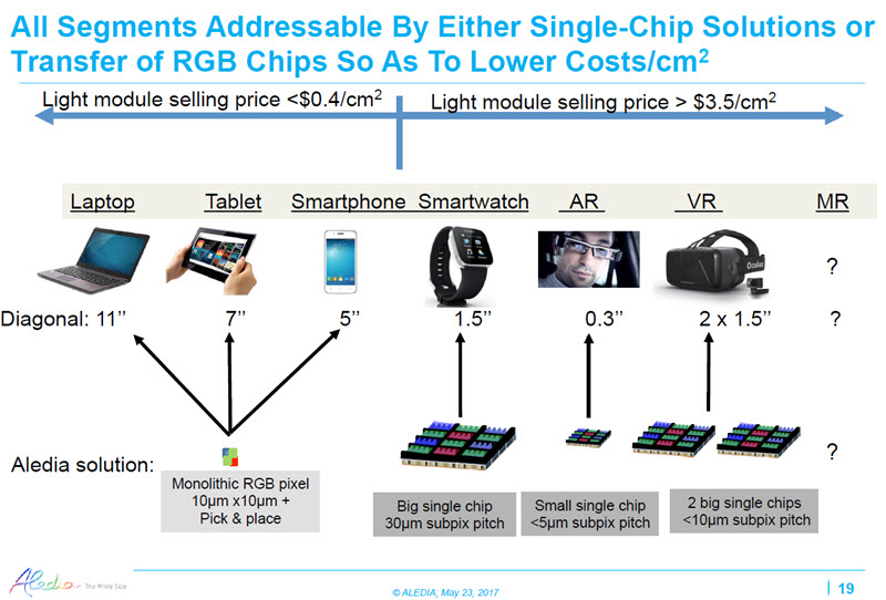
With costs of over $3.50 per sq cm, AR/VR and MR are possible applications using big single chips. For bigger displays for smartphones and bigger devices, you have to spread out the LEDs. Mixed Reality needs a lot of brightness and that is an opportunity for Aledia.
Moving to commercialisation, Aledia has a two step strategy
- Gen 1 will use blue emissions from the wires and use quantum dots for colour conversion of red and green
- Gen 2 will natively create RGB – Aledia started its developments with that approach and is now developing it again. Everything is done at the wafer level and development is around two years behind.
Gen 1 has very good colour gamut, but lifetime has been an issue, although it is getting a lot better. Gen 2 can get wavelengths down to around 700nm infrared, which will open up new applications and is said to be cheaper than QD-based solutions.
Gen 1 is suitable for displays at up to 2500 ppi – but there is a brightness limit to 10K cd/m² and is likely to be very useful for AR. Gen 2 may be able to get up to 6000 ppi and with brightness of more than 1 million cd/m². The technology can use interconnections based on copper to copper bonding from the semiconductor industry.
Many companies getting into microLED, but getting to the ‘7 nines’ level of yield will be a big challenge for them, Aledia believes. Moving forward, for Gen 1, the QDs need improvement but given the success of QD companies in other areas, it has been hard to get attention for microLED companies.
Gen 2 can use standard MOCVD and that means using standard CMOS foundries, which will be a big advantage.
The whole LED industry was built around a lab process that has been scaled up but hasn’t really changed, so it remains very tricky.
Up to now, the focus has been on getting a good blue – and Aledia said it may have the best EQE on the blue, but is not so advanced on red and green.
Analyst Comment
LETI has, of course, been working on emissive displays for a very long time, and we have been reporting on developments since 1998 (and it was already many years into research at that point). It has worked on FRDs and CNT-based FEDs. The Aledia claims are impressive and if it can get the attention of QD companies, as suggested above, to develop the colour conversion it needs and if its process is as straightforward for CMOS fabs as it claims, it could have a significant impact. (BR)