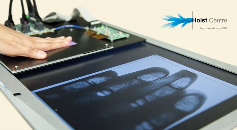
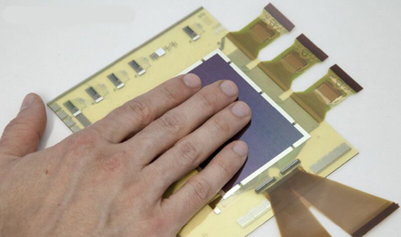
 Jon PeddieResearchers from the Holst Centre in Beligum, an open innovation initiative of IMEC and TNO in the Netherlands, have demonstrated a new class of flexible, large-area sensor technology for detecting finger and palm-prints. It is less than 0.2 mm thick and doesn’t use prisms or any moving parts.
The sensors can be built into mobile phones, notebooks or door handles to create an invisible and secure access control system. It can tell if the print is from a living person rather than a phantom or counterfeit — we never have to fear having our fingers cut off by terrorists again.
 Touch the screen anywhere, with one to four fingers.
The fingerprint sensors combine an organic photodiode front-plane, an oxide thin-film transistor (TFT) backplane (originally developed for flexible displays) and a thin-film barrier for protection against the environment. Holst says all three elements have been or are being transferred to industry for scale-up and commercialisation.
The sensors read the finger or palm-print by detecting visible light (400 to 700 nm) reflected from the surface of the skin. However, they can also detect light that penetrates someway into the skin before being reflected. This allows them to sense a heartbeat from changes in the capillaries within the hand and thus, verify that the print comes from a live person — similar to how a Fitbit or Apple Watch works.
By using different photodiode materials, the sensors’ capabilities can be extended to other wavelengths such as near infrared (NIR). This could enable new identification verification modes based on the pattern of veins in a hand, which is believed to be even more specific to an individual than a fingerprint. NIR sensors could also be used in other applications such as blood oxygenation monitoring, or for night-vision and 3D facial recognition — there’s a lot of interesting possibilities here.
 A panel as small as 6 × 8 cm can be used for identification. (Holst)
At SID Display Week in Los Angeles and the IMEC Technology Forum in Antwerp, Belgium, Holst showed that a 6 × 8 cm, 200-ppi panel is large enough for the four-finger scanners that are currently used by border control authorities, and delivers sufficient image quality for basic identification applications.
The company says that a slightly smaller, 500-ppi panel offers even higher image quality, sufficient by FBI standards and enough for law enforcement agencies to visualise minutia and pores, for more robust identification. IMEC is working on the read-out circuits for the prototype displays made by patterning thin-film photodetectors next to OLEDs. At least two smartphone makers are participating in the project.
Holst Centre was set up in 2005 by IMEC and TNO, and is supported by local, regional and national governments. Located on the High Tech Campus in Eindhoven, the Netherlands, the facility is an independent R&D centre that develops technologies for wireless autonomous sensor technologies and flexible electronics. It has over 200 employees from some 28 nations and a commitment from more than 50 industrial partners. For more information, visit www.holstcentre.com.
Analyst Comment
When I check in at passport control entering the US and put my fingers down on the Global Entry green finger pad, it seldom registers. After 11 to 13 hours in a dehumidified cabin, my fingers (and throat) are pretty dry, so the capacitive sensor doesn’t detect me very well. JP.
“Sorry, I can’t see you, go to the back of the line now.”
Holst’s optical technique will eliminate that problem, as well as give a more accurate measurement of the individual. We will see this in next-generation notebooks, phones and tablets, as well as some avant-garde commercial sites like point-of-sale checkouts, banks and even immigration services, one day. Finally, I can forget those damn passwords.

