Fraunhofer’s FEP (Institute for Organic Electronics, Electron Beam and Plasma Technology) is to present two papers at the forthcoming SID event on a new way of creating OLEDs with very high pixel density using an electron beam process. The process is applied after the OLED is created (including encapsulation). As a result of this, the OLED material itself can be unpatterned, which makes production easier. In a layered OLED structure, the individual layers can be modified. Flexible, glass-based or plastic OLEDs can be patterned.
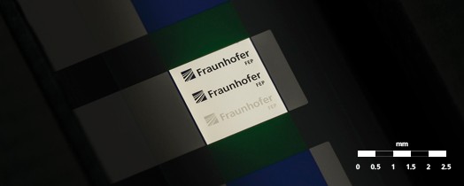
The institute said that even with a write time of less than two minutes, resolution of 12,700dpi could be achieved (2 µm spacing) and the display shown in the image was written in 100 seconds using a system from Raith GmbH, the manufacturer of nanofabrication systems. Work so far has been on monochrome OLEDs, but an enhancement to full-color patterning is being planned.

“Continuous gray scales in an image can be created on a monochrome OLED using the electron beam, while at the same time the local current consumption is reduced. The longer the dwell time on one spot with the beam, the darker the OLED will appear there”, explained Elisabeth Bodenstein from the development team at Fraunhofer FEP. “An impressive example is the white OLED shown, in which the image of the famous Dresden Semperoper was structured with the electron beam in a hundred seconds.”
Analyst Comment
Patterning of the materials efficiently and accurately is one of the challenges for OLED makers. (BR)

