 According to Fraunhofer FEP, OLED microdisplays are increasingly establishing themselves in consumer-ready wearables and data glasses. In order to meet the requirements for higher efficiency, higher contrast and higher resolutions in these applications, scientists have developed a new micropatterning approach for OLEDs on silicon substrates.
This might eliminate the use of colour filters and shadow masks in the future and allow full-colour displays to be developed. An increase in efficiency and considerably broader colour gamut have already been demonstrated in early experiments.
Since the launch of Pokémon Go, more people now know what AR means — additional interactive information interwoven into the real world. In addition to industrial use, medical technology and electronic entertainment, AR and VR applications have also been established in advertising and the education sector. Lightweight head-up displays can transform exhibitions by integrating film scenes, audio and other interactive content.
Thanks to the shallow overall depth that results from the self-luminous properties of OLEDs and their contrast ratio, manufacturers are increasingly turning to OLED microdisplays for AR/VR glasses. Fraunhofer FEP has been immersed in the development of this technology for several years. There are still some technological challenges that need to be mastered to exploit the full potential of OLED technology for use in consumer-ready data glasses and other AR/VR applications, such as brightness and efficiency, yields for large chip areas, curved surfaces, integrated eye-tracking and transparent substrates.
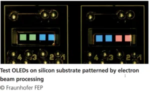
Currently, full-colour OLED displays can only be realised by using colour filters or patterned using shadow masks, which limit efficiency and resolution. Researchers are working on new approaches to fabricate high-resolution microdisplays while, at the same time, offering high efficiency and long operating life-time. The patterning of the organic layers of OLEDs is one of the greatest challenges, since conventional methods such as photolithography cannot be used with organic semiconductor materials. The use of electron beam technology for microstructuring was demonstrated at the Fraunhofer FEP two years ago (Fraunhofer Uses FEP to Boost OLED Resolution). Using its patented process, FEP was able to modify the emission of an OLED through the existing encapsulation layer to create any feature imaginable and even produce high-resolution greyscale images.
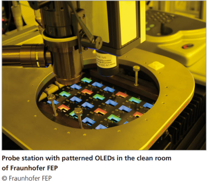
Further development of the electron beam process has now achieved full-colour OLED without using colour filters or shadow masks. To create red, green and blue pixels, an organic layer of the OLED itself is ablated by a thermal electron beam process. This patterning causes a change to the thickness of the layer stack, which makes the emission of different colours possible. This is a step towards the development of full-colour displays without the use of restrictive colour filters. Developer Elisabeth Bodenstein explains the advantages:
“W
ith our electron-beam process, it is possible to thermally structure even these sensitive organic materials without damaging the underlying layer”.
The results were obtained by simulating and initially estimating the hole transport layer (HTL) thicknesses that are produced by the electron beam. Researchers were able to decouple red, green and blue emissions from white OLED. These colours were demonstrated on the first test substrates, exhibiting comparable OLED performance.
In addition to using this new process for OLEDs, electron beam processing can also be used for other applications in organic electronics and inorganic layers. Moreover, the electron-beam patterning process is adaptable and can be employed in the areas of photovoltaics, MEMS and thin-film technology. Now, scientists are approaching new milestones, having completed promising preparatory work. The main goal in the coming years is to use this new method to develop fabrication of OLED microdisplays and establish it in the industry through licensing.
To do this, the features will be further miniaturised and the process optimised, through collaboration with industry partners. The next planned step is to integrate micropatterning into existing processes to gain further know-how.
In parallel, scientists are also planning enhanced simulation of OLEDs. The OLED colour spectrum will be broadened by modifying materials and layer thicknesses. The incorporation of displays in data glasses for applications such as industrial manufacturing and medicine should be opened up by the new process. Scientists are ready for advanced development of the technology through partnerships and joint projects with display, plant, material and system manufacturers. The results and first coloured OLEDs will be presented during IMID 2018 in Busan, South Korea, which takes place between August 29th and 31st.