One of the fun things about taking an interest in displays is that there are such a wide variety of technologies and topics that are relevant, from materials science, semiconductors, optics, electronics, mechanics, environment, business and human factors. Of course, nobody is an expert in all these things (although some of our Display Daily writers give a good sense that they are!).

Today, I’m going to step outside my comfort zone and mention a company that is based in Silicon Valley and is working in the LED field, Verticle Inc. It is, apparently, 16 years old, but seems to have been in stealth mode for a long time. In a look around the web, I found little about the company, apart from a list of patents. I’m not a semiconductor engineer, or LED expert, but I thought that what the company is developing is very interesting.
Now, as Sweta wrote earlier this week, miniLED is a really interesting development in LCD backlights, but the technology needs lower cost miniLEDs to allow more to be used. MiniLED-Based Displays Poised for Expanded Presence)
Cost Reduction
Verticle pointed out that shrinking the LED die size is one of the most effective ways to reduce the manufacturing cost. However, the firm says, the opportunity to shrink die size is limited with current die singulation technologies (e.g. the industry standard laser dicing process) due, it says, to chip damage and extremely long processing times. This is particularly true for LED dies less than 100µm.
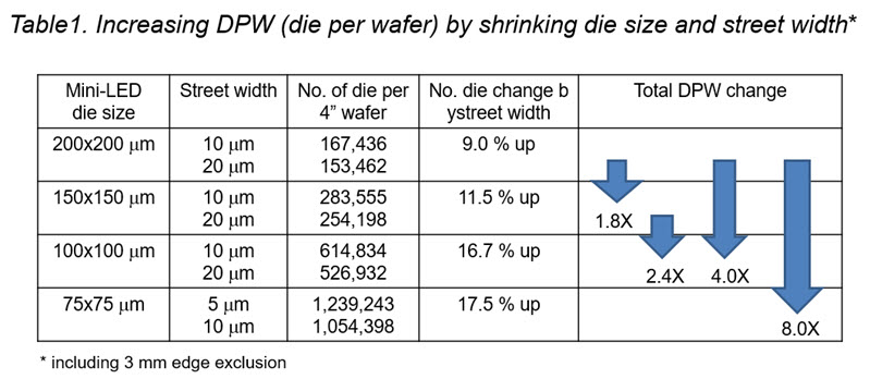
The company has an innovative die singulation technology, “Chemical Dicing”, that is claimed to enable a reduction in miniLED die size without chip damage. Using the chemical dicing process, the firm said that dramatic cost reduction can be achieved by a substantial increase in die count per wafer. Furthermore, as shown in Table1, it can result in narrower street scribe width as well.
The damage-free nature of the chemical dicing is important as it separates the die by wet chemical etching the street line instead of thermal or mechanical methods which generate heat or acoustic shock waves. As a result, there is no damage around the chip edge, Verticle says, which means that the distance between active areas and chip cutting edges can be less than 2 µm. Therefore, the active area can be enlarged which results in more light output from the same size LED die. And, of course, that means reducing cost.
As shown in Table 1, die size shrinking and street narrowing yield dramatic DPW (die per wafer) increases by up to 8X as compared with conventional flip-chip based miniLEDs which have larger die sizes and wider street widths.
Why Should LEDs be Rectangular?
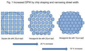
The firm pointed out that additional DPW increase can also be obtained by chip shaping. Unlike conventional die singulation methods that can only separate die in a linear direction (i.e. only able to separate either square or rectangular die), chemical dicing enables free-shape die (e.g. hexagonal) formation and singulation. Fabricating a hexagonal die can increase DPW by more than 20% due to enhanced tiling efficiency and increased usable wafer area (Fig.1).
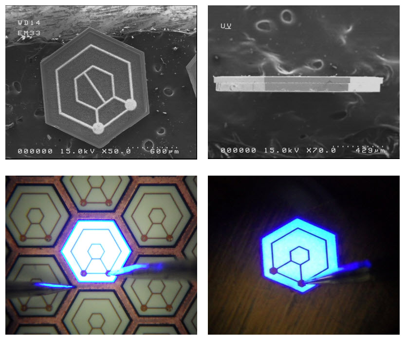
Using this unique chemical dicing, Verticle said it was able to fabricate hexagonal die for the first time in the world (Fig. 2). The hexagonal shape symmetry can help better current spreading, which results in higher light output than square or rectangular die, it claims. Additionally, hexagonal die light output is enhanced after packaging as well. A hexagonal die produces a beam profile which is much closer to the circular shape of circular lenses used in optics design. In contrast, the beam profile of the more usual square or rectangular die, when combined with circular lens, is typically distorted.
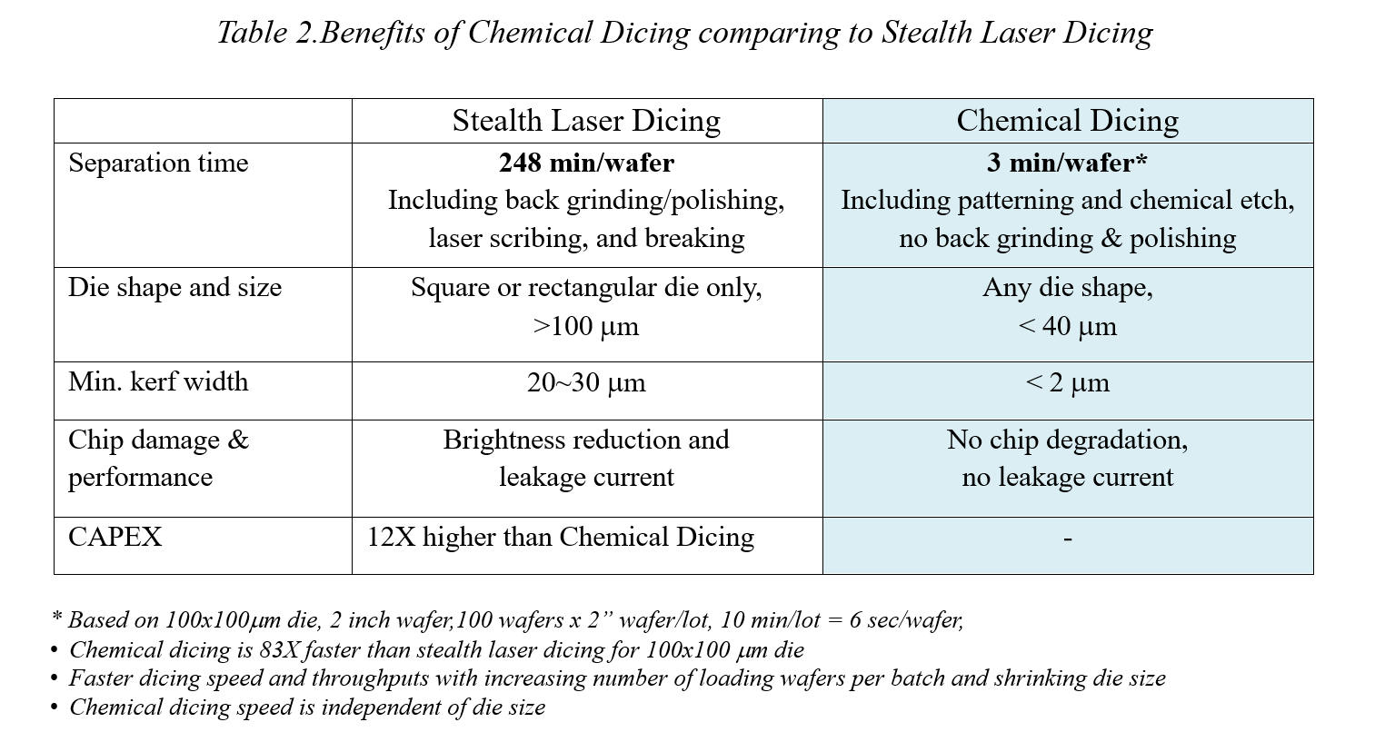
Moreover, Verticle told us, multiple wafers in one batch can be etched simultaneously, resulting in die singulation throughputs which are 500X greater than stealth laser dicing (Table 2).
Now, I’m not enough of an expert to spot if there is a ‘gotcha’ to the very interesting claims of Verticle, but would welcome comments and feedback from readers! If you want to contact the firm, the CEO (and patent listee) is Myung Cheol (‘Mike’) Yoo ([email protected]) (BR)