Alain Harrus, CEO of Kateeva left the company, replaced by May Su, previously responsible for strategic planning. Kateeva was a start-up founded in 2004 by Conor Madigan who worked on the concept of Ink Jet Printing (IJP) at MIT, in the same group that spawned QD start-up QD Vision, founded by Seth Coe-Sullivan.

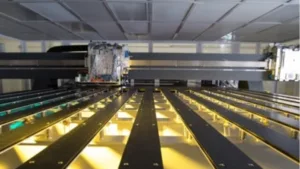
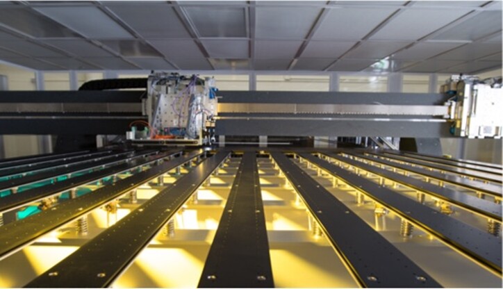
Theorectically, IJP of organic material was a natural. By IJP a soluble organic material, either polymer or small molecule, no mask was required, material utilization would be >90% compared to <50% for VTE, the placement would be precise, and the capital costs would be lower. Ink jet heads have been under development for years, so they were finally ready to meet the tight specs needed to print sub-pixels. The printers are enormous, designed for Gen 8.5 fabs to print TV size panels. Small/medium size panels for smartphones required 400+ppi, which was outside the parameters of IJP at the time. While the printing was perfected, soluble emitter material, either small molecule in solution or polymer was inferior to phosphorescent dopants used to manufacture OLEDs, so the application lagged.
However, with the adoption of flexible displays, the encapsulation method that used two glass substrates with a frit adhesive was replaced with some form of thin film. Samsung, the developer of flexible displays chose a combination of 1 organic layer surrounded by 2 inorganic layers for TFE and chose Applied Materials to deposit the inorganic layers and Kateeva to print the organic layer.
The organic layer contributed to the moisture barrier and also served as a planarization layer. Kateeva was ‘off to the races’ and other panel makers adopted the Samsung solution creating a significant business for machines as the tools for the TFE stack cost $85 million (1 printer + 2 PECVD tools – corrected from original version). In 2020, Kateeva had an opportunity for growth as Chinese panel makers and Samsung looked to OLED flexible displays as the future, with a potential additional demand for 20 tools. Competitors; Panasonic, SEMES and TEL were also eyeing this opportunity, which could exceed $2b, plus service contracts.
Table 1: Future Gen 6 Installs, Capacity and IJP for TFE  Source: APS, Hana Securities, OLED-A
The original purpose of IJP was to print sub-pixels and change the cost dynamics of OLED displays. LGD, SDC, CSoT, JOLED and BOE researched the use of printed pixels. Samsung decided to go with QD 1.0, vacuum depositing blue OLED layers and printing red and green QD color converters. They built a Gen 8.5 pilot line with Kateeva printers and started testing the process. The results were promising, and Samsung planned to roll out the first production line of 30K Gen 8.5 substrates/mo. in Q121. Kateeva saw this as another $1b opportunity, a potential IPO and doubled its staff to support the effort.
Kateeva Hits a Glitch
Three months ago, Kateeva laid off half of its staff, including the COO, CTO and other executives, because Samsung awarded the QD 1.0 contract for the IJP to SEMES a Samsung owned company with 2 divisions, one for semiconductor equipment and one for display equipment, While the semiconductor division was successful, the display division, which concentrated on LCDs was failing and the company had been unsuccessful in finding a buyer. But SEMES had invested in IJP for LCD color filters and believed that they could exploit these efforts to print QDs for QD 1.0. The competition was a no-brainer as SEMES equipment couldn’t meet the performance spec. But performance is not always the final decision point. Samsung was already looking at another use of IJP for GaN nano rods and decided that the technology was a fundamental component of their long term display strategy. They were already being deposed in the LCD business by the Chinese. How to protect their franchise?
If Samsung awarded the contract to Kateeva, the company would push their technology to Chinese panel makers. If Samsung bought Kateeva, they worried that the key employees would eventually leave and re-create the technology to sell tools to the Chinese. The SEMES executives, former SDC and SEC VPs lobbied with former colleagues in the all-powerful Chairman’s Office that they could produce a comparable tool and basically made a deal with the devil by pricing it at ½ of the Kateeva price (corrected from ¼ in the original article – Editor). In comes SEMES, out goes the Kateeva IPO and 50% of the staff. Kateeva gets working capital from an existing Chinese private equity investor but they needed to get their pound of flesh, so out goes Alain.
Why couldn’t Kateeva be rescued by one of the other panel makers investing in OLED TVs:
- LG already has 2 Gen 8.5 fabs for OLED TV panels and felt that the process was more cost effective using Chinese capital for the Guangzhou fab, and switching to a top emission solution, which increased the aperture ratio and the associated luminance. LGD was also in the throes of closing their LCD fabs, which in the short run would reduce the revenue stream and their plans for a Gen 10.5 OLED fab were on hold.
- BOE is apparently cooperating with LG as the company understands the cost dynamics of Chinese investment and sees RGBW as the quickest and least risky play to enter the market
- JOLED has already committed to using polymers and the Panasonic tool and redesigned their approach to print lines instead to sub-pixels to get the best color point from the underperforming polymer material.
- TCL is undecided but is likely to work with JOLED for a proven solution to minimize risk and speed up entry into the market. JOLED would like to build and operate the fab for TCL in Japan, but TCL wants the economic benefits of a Chinese location and the experience of CSoT.
Since the mid-2000s, Samsung been the creative leader of the display industry in technology, capital expenditures and revenue, but is now challenged by BOE and CSoT. During that time, they pioneered the growth of substrate sizes from Gen 4.5 to Gen 8.5, forged the use of LED backlights and QD color converters, and single handedly pioneered the OLED small/medium business (including flexible displays) from scratch to over $20b in annual revenue. But like any innovator, it was not without missteps, the Note 7, the pre-release of the Galaxy Fold and the pass on buying UDC at less than 1/10th its current market cap to name a few. But engineers on the IJP project have said “This is the worst decision Samsung has ever made”. Samsung’s Gen 8.5 QD 1.0 pilot is producing 100s of good panels per week, while the SEMES tool struggles. It is likely that Samsung’s highly talented engineers will make it work, but much is on the line, for in QD 1.0, only the QDs are printed, but in QD 2.0, the QDs and the nano rods must be printed and aligned at yields exceeding 99.9999%. Meanwhile Kateeva, which could be viewed as insurance has lost much of the talent to step in quickly if called upon. (BY)
Barry Young is the Chairman and CEO of the OLED Association