Quantum dots (QDs) are exactly that – microscopic balls of material that are roughly spherical and practically zero-dimensional points. Quantum dots have been hailed as a technology that can bring near-Rec. 2020 colorimetry to consumer systems. On the other hand, startup Verlase Technologies LLC has technology targeting the same markets as QDs but based on planar two-dimensional thin layers of material.

Verlase has three recently issued US Patents:
- US 9,035,344 titled “Phosphors for use with LEDs and other optoelectronic devices.” Issued May 19, 2015
- US 9,019,595 titled “Resonator-enhanced optoelectronic devices and methods of making same” issued April 28, 2015.
- US 8,859,412 titled “Optoelectronic device containing at least one active device layer having a wurtzite crystal structure, and methods of making same” issued October 14, 2014.
All three of these patents list Ajaykumar R. Jain, the CTO of Verlase, as the sole inventor and are assigned to Verlase. According to George Powch, President/CEO of both Verlase and its parent company Versatilis, a fourth patent should issue soon.
The ‘344 patent and the ‘595 patent relate to distinctly different technologies, although they are both related to large 2D areas rather than essentially 0D dots.

In the ‘344 patent, they take a semiconducting material, like graphene, which grows in weakly-bound crystalline layers. This material can be exfoliated into very thin layers. Further processing of these thin layers controls the thickness and/or the materials of the thin layers, which controlling the bandgap energy and Quantum Well (QW) thickness and therefore the wavelength of the materials. This exfoliating approach is described in the ‘344 patent.
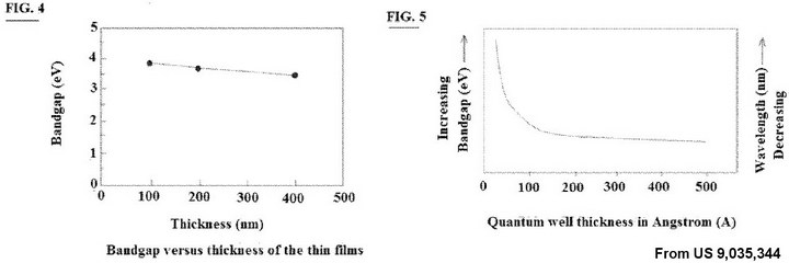
According to the company, they have developed a roll-to-roll approach to handing these materials. Figures 4 and 5 from the ‘344 patent show the thickness of these thin layers, called nano platelets, determines the band gap of the material and the band gap then determines the emission wavelength of the material. In use, these materials would replace conventional phosphors to absorb blue light from a LED and convert it to green or red light (or some other color), depending on the design of nano platelets.
Powch told me, “…besides exfoliating 2D materials into nano platelets as QWs, they can also be grown levering existing semiconductor industry capabilities, for lower costs and very precise control of the process. This also plays into enabling certain 2D semiconductor materials as electroluminescent layers in LED-type devices that can directly emit most any color in the visible, something QDs have yet to do commercially.”
According to Powch, the holy grail for this technology is to use these materials as an EL layer with charge injection layers. He says, “We showed this crudely, and have a patent coming out shortly. In that case, these 2D materials can be grown in a conventional fab, and on Silicon!”

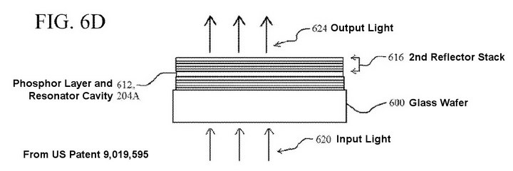
The second approach, covered by the ‘595 patent, is to produce resonators with layers manufactured by using MBE of II-VI materials, semiconductor processing and optical thin film manufacturing technologies. These technologies are very well developed, except MBE of II-VI materials, which should make this Verlase technology easy to implement in production. Most current MBE technology for displays uses III-V materials such as GaN or GaAs. All of these three key technologies can be done on a wafer scale, allowing the Verlase resonator technology to also be wafer scale. Unfortunately, this cannot be done on the LED or laser wafer but is done on a separate glass wafer, as shown in Figure 6D from the ‘595 patent.
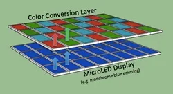
Patterned Verlase Color Conversion Layer used with a MicroLED Display in an NTE Application.
He added that these resonator cavities can be used either as wavelength conversion systems for LEDs or as an optically pumped semiconductor (OPS) vertical cavity surface emitting laser (VCSEL) or something “in-between.” This in-between system will look much like a Superluminous LED (SLD). Powch noted that while Verlase has demonstrated both wavelength conversion LEDs and OPS-VCSELs, they have not yet demonstrated these in-between systems.
I have looked at SLDs for display applications in the past and they have a number of very good properties. First, they have a narrow enough bandwidth to provide very good colorimetry, but still a wide enough bandwidth to eliminate all speckle. Second, a SLD can produce collimated light, not as collimated as a laser but more collimated than a conventional LED. Past SLDs I have examined had two overwhelming problems that have kept them out of displays – low output and high cost. Perhaps the SLD-like properties of these wafer scale in-between devices from Verlase will eliminate these two objections.
When I asked him about the efficiency of these systems, Powch told me, “Recall we are discussing two separate technologies. For QW nano platelets as phosphors (the ‘344 patent), IQE should be theoretically similar to QDs, but we think net useful photons from a practical system can be much greater if engineered correctly.
“For LEDs and lasers, that’s a completely different approach (resonator [as shown in the ‘595 patent]) and would have much higher conversion efficiency than any other approach we know.”
I’m running out of room and haven’t even gotten to the third Verlase patent, US 8,859,412. So I’ll let someone else describe its importance. “This is a key innovation for several important applications,” stated Professor Maria Tamargo, Professor of Chemistry at the City College of the City University of New York, and a leading expert on II-VI materials and devices. She added that “VerLASE has shown for the first time a novel, commercially feasible way to grow Wurtzite phase II-VI crystal films, a focus area of research worldwide”
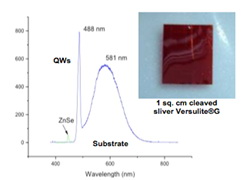
 Properties of Wurtzite from Verlase
Verlase Technologies LLC (http://www.verlase.com/) is a January 2013 spin-out from Versatilis LLC (http://www.versatls.com). Versatilis retains a majority interest in Verlase, with a first private investment round led by Wakley Limited. The spin-out leverages years of R&D by the company’s principals in advanced materials and processes for enabling semiconductor devices on large area, flexible substrates. Powch says about the Verlase business model, “We would definitely partner with bigger companies for channels to market, whether licensing or other forms of engagement, and depending which technology and application space is involved. We may pursue certain niches by ourselves – it is possible to outsource much of the manufacturing, as we have been doing during development.”
Versatilis was founded in 2004 and commercializes technology through spinning out market focused new ventures, and by selling and licensing technology to others. The company is funded by a number of private investors who specialize in leading edge technology ventures with a significant intellectual property (IP) portfolio. –Matthew Brennesholtz

