Mike Spaid, President and CEO of what is now Cambrios Advanced Materials, joined its predecessor company (Cambrios Technologies Corp.) in 2005, shortly after that company was founded. That was also the year Cambrios first demonstrated its silver nanowire (AgNW or SNW) ink and set out to displace indium tin oxide (ITO) as the leading transparent conductor.

Cambrios found customers, including Lenovo for an all-in-one PC, Toshiba for a touch-screen laptop, and Crystalsol for photovoltaic cells. But the company, along with its direct competitors, found the need for capital to move forward seriously outstripped its revenues and ability to raise funds. Cambrios eventually found itself in the humiliating position of selling off its assets at auction.
In an email interview Mike Spaid continued the story:
“Cambrios went through an ABC process (assignment for the benefit of creditors) in which the company’s assets including its patent portfolio, know-how, and equipment were acquired by Champ Great International, the family fund of Michael Chiang (Chairman of TPK). Mr. Chiang was the single largest private investor into Cambrios and a true believer in the technology and its value to the consumer electronics market. In May 2016, a new entity, Cambrios Advanced Materials Corporation was formed in Sunnyvale, California, with the original core R&D staff focused on continued development and improvement of silver nanowire materials. In early 2017, Cambrios Film Solutions Taiwan was formed with the key functions of sales and scaled manufacturing of silver nanowire materials. In addition to Cambrios Film Solutions Taiwan, an ink formulation facility was established in China. Now a global company with R&D in the US, scaled nanowire synthesis in Taiwan, and final ink formulation in China, Cambrios required one more step to complete the supply chain: SNW based films. Most recently, Cambrios has established key relationships with industry leaders capable of volume manufacturing of coated film in Japan, Korea, and China. Whereas Cambrios prior to its new management was focused on selling ink, under new management the company has moved further down the supply chain to provide novel films to its key customers.”
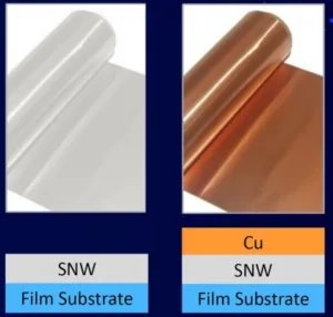
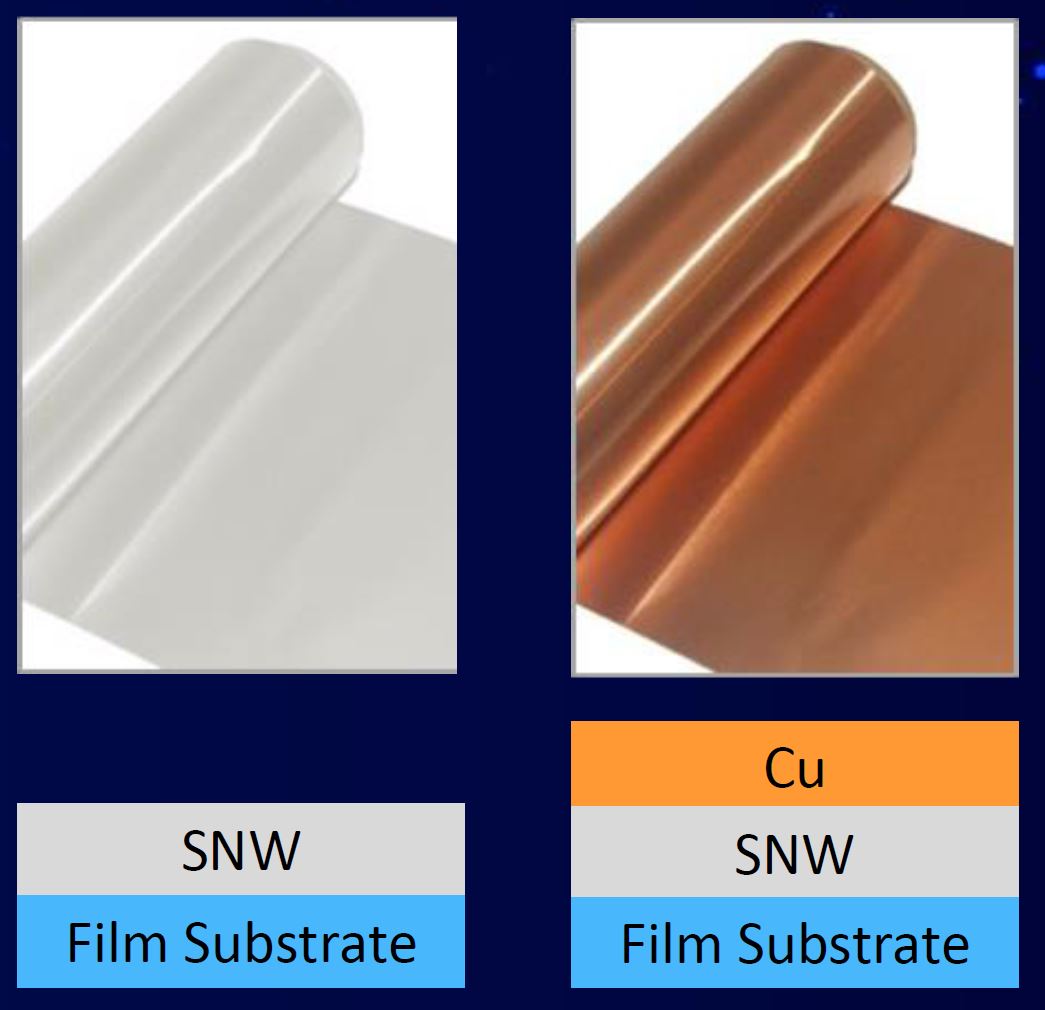
In a recent press release, Cambrios highlighted its MOS (metal on silver nanowire) film. In MOS film, the SNW ink is applied to the film via slot die in the normal way, but then a layer of copper is sputtered over the SNW. But SNW is already a conductor. Why add the copper? Again, Mike Spaid:
“Copper is used to electrically connect the transparent conductive layers to the chip that drives the touch sensor. Although SNW is an excellent conductor, the wiring in the bezel area needs to be patterned on a very fine pitch to produce an extremely narrow bezel (essentially no visible bezel), allowing the display to span the entire device surface. Zero bezel designs require 10 micron wide conductive lines with a 10 micron space between adjacent conductors. To minimize the electrical resistance in the wiring from the transparent conductive pattern to the chip, the material needs to be a few orders of magnitude more conductive than the SNW transparent conductive layer. This level of conductivity can only be achieved by a continuous metal film, such as copper. Cambrios has integrated the transparent conductive layer comprising the touch sensor and the key wiring layer in a single film, allowing for the sensor pattern and the bezel pattern to be produced using a single material.”
It seems that Cambrios is not only preaching to the converted. Its MOS film won the Flexible Display Material of the Year Special Contribution Award at 2019 Display China.
The Cambrios SNW ink was always impressive. Now, with an enthusiastic and deep-pocketed investor, and with control of an extended supply chain that brings the company’s products closer to the ultimate customer, we can safely say the phoenix is spreading its wings. We have yet to see how high it can fly. – Ken Werner
 The Cambrios MOS film consists of the company’s standard silver nanowire film with a sputtered layer of copper. (Photos: Cambrios)
Ken Werner is Principal of Nutmeg Consultants, specializing in the display industry, manufacturing, technology, and applications, including mobile devices, automotive, and television. He consults for attorneys, investment analysts, and companies re-positioning themselves within the display industry or using displays in their products. He is the 2017 recipient of the Society for Information Display’s Lewis and Beatrice Winner Award. You can reach him at [email protected] or www.nutmegconsultants.com.