This week I was in Grenoble in the Alps and took the chance to visit Leti, the major French R&D. At the exhibition, I also caught up with a LETI spin-off, Aledia, which has a novel approach to microLEDs.

Leti is one of the main semiconductor research organisations in mainland Europe, alongside the Fraunhofer IPMS and IMEC. At the event this week, when Leti celebrated fifty years of operation, the organisation announced an agreement with the Fraunhofer IPMS to work together. Europe is basically out of the race in mainstream CMOS and FinFET chip making, but has a strong position in power electronics, sensors and the strategy for the future is to focus on power electronics, chips for the IoT and for autonomous vehicles. The aim is to focus the R&D effort on technologies that can support the areas where Europe is strong, such as the automotive industry.
Leti focuses on R&D and once technology is developed it either contracts for technology transfer or sets up spin-offs. An early spin off was STMicrolectronics, but there have been many over the years. We’ll have an in depth report on this in our subscriber news, but for now, let’s focus on Aledia.
The company’s approach is based on making GaN nanotubes to create LEDs. The GaN material can be deposited by Aledia on silicon wafers rather than the sapphire wafers used by other LED approaches. Although GaN is used, there is a lot less used than on traditional LEDs.
At the recent SID Investor’s Conference, Aledia gave a talk (it has around $40 million of funding) and claimed that its LEDs are three times cheaper than regular GaN LEDs. Further, the technology can be used to make nanowires on 200mm wafers and could even go up to 300mm, which means that regular semiconductor equipment can be used.
Aledia’s ‘secret sauce’ is to be able to make the nanotubes at a very even length – apparently this is very tricky, but critical for good uniformity. One of the key advantages of the technique is that the nanowires are very tiny indeed. That means that even on a small device there are very many tubes, so if a few fail, the performance doesn’t suffer – Aledia calls this built-in redundancy.
Aledia can make very large area LEDs and that may have applications in special areas including lighting but the aim is to build displays based on microLEDs that are on top of control circuits that can be down to 3 microns square and may even go down to one micron. Of course, like other microLEDs, you could cut the chips up and distribute them over a large area. However, the initial market is for small monolithic displays, where the high brightness and efficiency are obvious advantages.
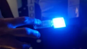
 Aledia showed this big LED in Grenoble – it’s a single diode, not an array. Image:Meko
Near to eye displays in augmented reality (AR) applications really need very high brightness and high efficiency and that makes this kind of application attractive. The high brightness is important because in AR the display has to compete with sunlight. Furthermore, the optical systems are of low efficiency, so the source has to be very bright. The efficiency is important to reduce the power needed for headsets.
At the moment, the displays have been developed to produce blue light, although in Grenoble, a white sample was shown, using phosphors for colour conversion. Full colour displays can be made using Quantum dots or phosphors, although there are challenges in lifetime and brightness is more limited than with the wires alone because of the heat.
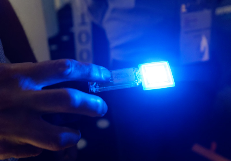
 Aledia showed this white LED using phosphor for colour conversion. Image:Meko
In the future, the wires can be tuned to create other colours (apparently right down to infrared wavelengths). Isn’t it simpler to use colour conversion, we asked? That would avoid issues of different colour performance over the life of the display and at different temperatures. However, this is not a problem for Aledia, as, unlike other LEDs, the same materials and structures are used for all the colours, so differential issues are not expected to be an issue.
Leti is also working on ‘traditional’ GaN LED microdisplays and we will have a report on those in our subscription MDM newsletter this week. – Bob Raikes