A team of researchers at Zhejiang University (Hangzhou, China) are developing a laser-driven, programmable, non-contact transfer printing technique that could be applicable to the transfer of microLEDs. The technique is based on the use of an active, elastomeric, micro-structured stamp with tunable adhesion.

First a few words of background information.
Transfer printing is an assembly technique that can be used to transfer micro-objects including inks, micro-scale Si platelets and, most relevant to this article, microLED chips. The transfer is from a donor substrate to a receiver substrate and is accomplished by the use of a soft, polymer stamp. Note in particular that the receiver can be a “challenging flat or rough” substrate. Of relevance to electronic displays, this includes flexible and/or stretchable receiver substrate materials. Successful use of this technique could enable transfers at the rate of thousands of micro-objects per second.
Various approaches to transfer printing have been investigated based on tunable dry adhesives using both contact and non-contact techniques. In both techniques, accomplishing the transfer depends on the ability to switch adhesion between the stamp and the micro-object from a strong picking state to a weak printing state. It follows that one goal to implement transfer printing is to actively and reliably manipulate interfacial adhesion between the stamp and the micro-object.
As a practical matter, contact techniques have been found to be very sensitive to the geometry and properties of the receiving substrate. Non-contact approaches, on the other hand, eliminate the influence of the receiver on the transfer yield and allow non-contact printing of micro-objects onto arbitrary receivers. Unfortunately, existing non-contact transfer printing techniques usually induce undesired high temperature increases in the system. This, in turn, may cause permanent interfacial damages thus preventing the use of the process in the transfer printing of brittle materials.
To address these issues, the researchers investigated a laser-driven programmable non-contact transfer printing technique. A recent article on this topic is entitled “Laser-Driven Programmable Non-Contact Transfer Printing of Objects onto Arbitrary Receivers via an Active Elastomeric Micro-Structured Stamp.” It was published in National Science Review, nwz109. A copy of the article is available for download and can be found here.
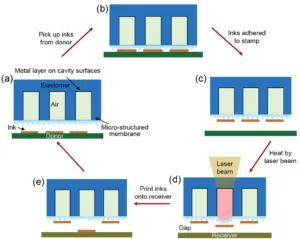
Paraphrasing the description in their article, the approach developed by the team is described as using an active elastomeric micro-structured stamp that can be thought of as a tunable adhesive. It is based on cavities filled with air and encapsulated by a micro-patterned surface membrane. The micro-patterned surface membrane can be inflated dynamically to control the interfacial adhesion. This is done by using a laser to heat the air in the cavities. The heating process is implemented by use of a metal layer (such as iron particles) on the inner cavity of the surface that acts as an absorbing layer.
The transfer process is illustrated in the figure below. The figure and the descriptive text are drawn from the article cited above. (Note that, in the example used in the figure, the material transferred is an ink rather than a microLED chip.)
Schematic illustration of the laser-driven programmable non-contact transfer printing process via an active elastomeric micro-structured stamp.
- The stamp is moved above the donor substrate.
- The stamp is in contact with inks by a light pressure with the surface micro-tips collapsed.
- The rapid retraction retrieves inks onto the stamp with the surface micro-tips recovered.
- The inked stamp is moved on top of the receiver substrate, leaving a small gap between the stamp and the receiver. A programmable laser beam is used to heat the air in stamp cavities, which induces pressures on the micro-structured stamp membranes to facilitate the delamination of inks from the stamp.
- The removal of the stamp completes the transfer printing process. Inks on the unheated region remain on the stamp while those on the heated region are printed onto the receiver substrate.
Translation of the receiver substrate or scanning of the laser beam enables the formation of a desired pattern.
Theoretical and experimental studies discussed in their article report on the fundamental aspects of the design and fabrication of the active elastomeric micro-structured stamp, and the operation of non-contact transfer printing.
The approach was found to offer continuously thermal controlled tunable adhesion with of more than three orders of magnitude. The associated temperature increase was less than 100 °C.
The researchers conclude their article by claiming that “The fabrication of the adhesive bypasses the complex lithographic processes and provides a cost-effective route to realize the active elastomeric micro-structured stamp.” They go on to explain that their “innovative laser-driven non-contact transfer printing technique creates engineering opportunities in a wide range of applications including microLED display, where the heterogeneous integration of diverse materials is required.” -Arthur Berman
Zhejiang University, Jizhou Song, [email protected]

