
A team of researchers headed by Maria Baeva of Alferov University (St. Petersburg, Russia) is developing a light emitting perovskite-based electrochemical cell. It has a novel design and is claimed to have several advantages over conventional cells of this type.
Here is a few words of background information.
Conventional halide perovskite-based light emitting devices have properties that make them highly desirable for use in display applications. These properties include high efficiency, high color purity and a wide color gamut. Unfortunately, when attempting to fabricate such devices, there are inevitable and significant manufacturing problems. Part of the reason for these problems can be attributed to the complex, multilayer structure of the device. An additional problem becomes apparent when the device is in operation – poor stability due to heating.
One approach with potential to address these problems is the use of halide perovskite light emitting electrochemical cells. This type of perovskite optoelectronic device differs from conventional perovskite light emitting devices by being based on a simple, monolayer architecture.
The operating principle of perovskite light emitting electrochemical cells can be describes as follows. An electrical bias is applied to the device (basically a diode). Mobile positive and negative ions inside of the perovskite layer migrate towards corresponding electrodes. Doing so dynamically forms a p-i-n structure inside of the perovskite layer. This, in turn, allows effective electron-hole recombination with the emission of light.
A recent article by the team, referenced below, on their research into utilizing an approach based on an electrochemical cell is entitled “ITO-free silicon-integrated perovskite electrochemical cell for light-emission and light-detection.”
In this article, the team reports on perovskite light emitting electrochemical cells that consist of a silicon substrate, a multifunctional single composite perovskite layer (a mixture of halide perovskite microcrystals, polymer support matrix and added mobile ions) and a transparent single walled carbon nanotube film top contact. The configuration of the proposed device is illustrated in the figure below and on the right. The figure to the left is included for comparison and is a conventional device.
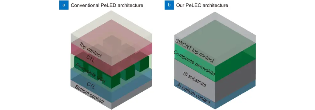
Due to silicon’s good thermal conductivity, it is found that a perovskite electrochemical cell with a composition of CsPbBr3:PEO:LiTFSI and fabricated on a silicon substrate with a transparent, single walled carbon nanotube film as a top contact exhibits 40% lower Joule heating compared to the perovskite optoelectronic devices fabricated on conventional ITO/glass substrates. Moreover, when a positive bias is applied to the device it yields a luminance of more than 7000 cd/m2 at 523 nm. The electroluminescent efficiency is 1.3×10⁵ lm/W.
It should be mentioned that, when a negative bias is applied to the device, it operates as a photodetector.
The technological potential of the new device configuration was demonstrated by fabrication of a prototype display composed of 24 pixel. The prototype further demonstrated the potential for device miniaturization by the creation of electroluminescent images with features smaller than 50 μm.
The researchers made a point of explaining the significance of the use of silicon in their device design. They state that “silicon is fundamental in CMOS semiconductor technology and that the integration of such an emerging material like perovskite material along with silicon brings the R&D community one step closer to obtaining an industrial perovskite light emitting electrochemical cell.”
An additional feature of the new approach is that the transparent electrode in the device does not use ITO. This is significant because indium (the I in ITO) is becoming scarce. It follows that its replacement by single walled carbon nanotubes, a more readily available material, is desirable.
The researchers conclude their article by admitting the need for further optimization of their new technology. Mention was made of two specific areas where improvement is needed: optical interface engineering between the Si and perovskite layers and device electrical stability improvement via transport and/or the introduction of passivation layers.
Reference
Baeva M, Gets D, Polushkin A, Vorobyov A, Goltaev A et al. ITO-free silicon-integrated perovskite electrochemical cell for light-emission and light-detection. Opto-Electron Adv 6, 220154 (2023). doi: 10.29026/oea.2023.220154